Light-emitting device and manufacturing method therefor

a technology of light-emitting devices and manufacturing methods, which is applied in the direction of semiconductor devices, basic electric elements, electrical apparatus, etc., can solve the problems of degrading luminous efficiency, affecting the light-emitting efficiency, so as to improve the optical characteristic of the light-emitting device, improve the light-emission efficiency, and increase the size of the uneven portion

Active Publication Date: 2018-05-17
SUZHOU LEKIN SEMICON CO LTD
View PDF5 Cites 1 Cited by
  • Summary
  • Abstract
  • Description
  • Claims
  • Application Information

AI Technical Summary

Benefits of technology

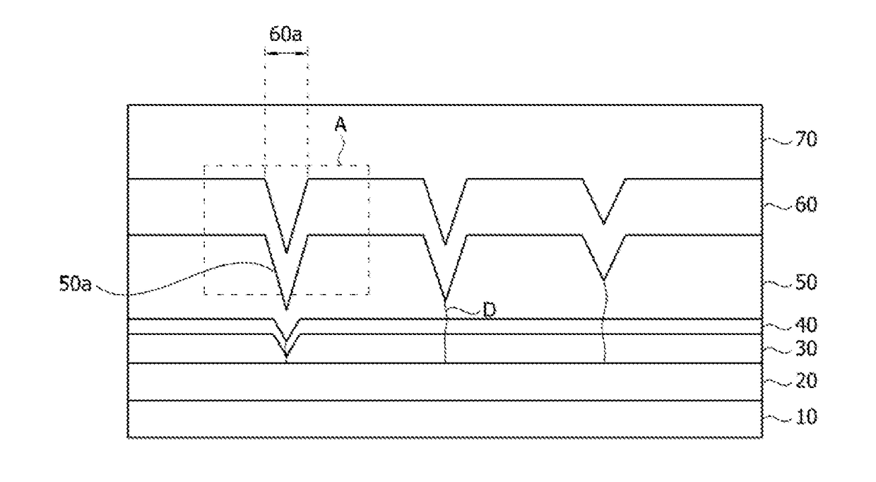
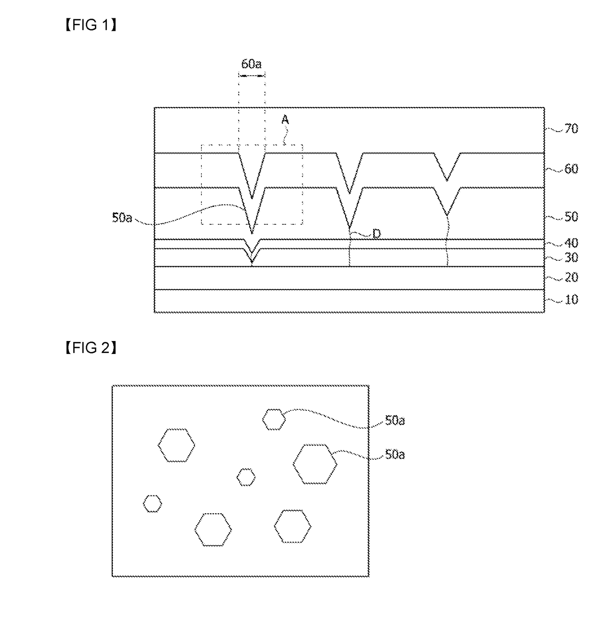
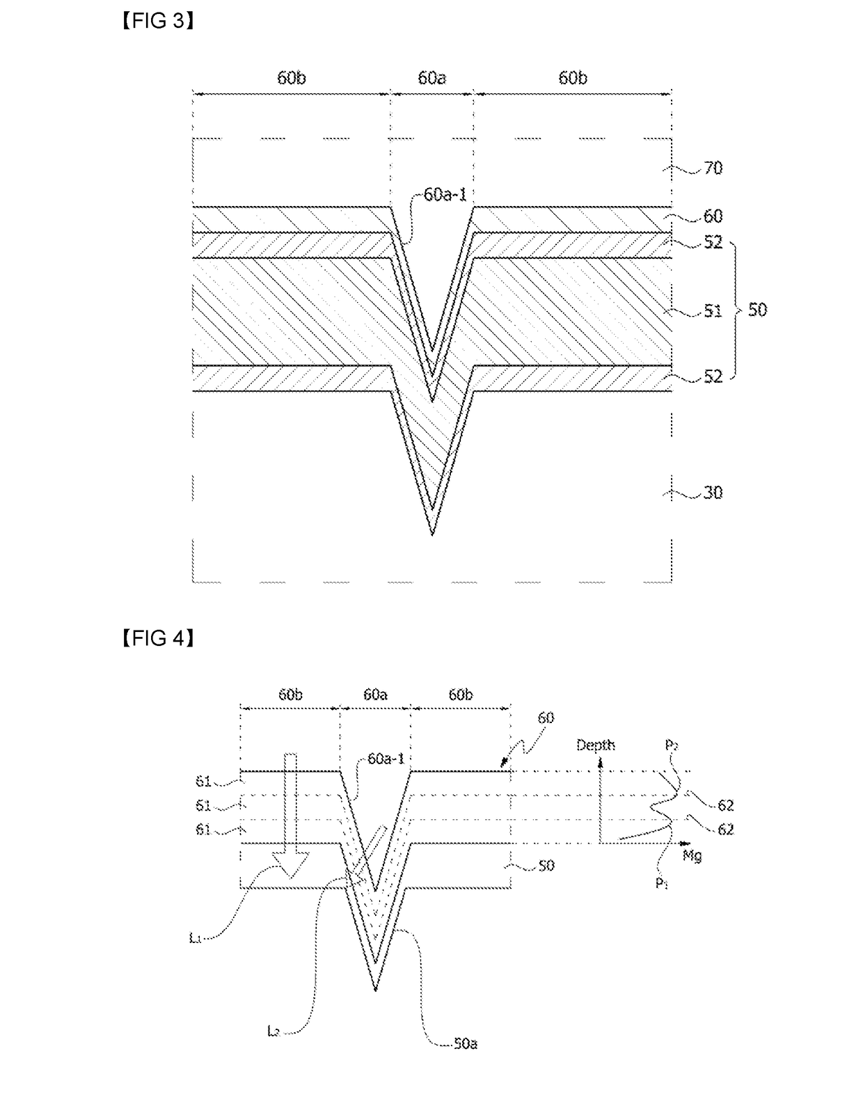
[0021]In accordance with the embodiments of the present disclosure, holes can be effectively implanted through a sidewall of a second uneven portion of an electron blocking layer. Therefore, even though a size of the uneven portion is increased, an optical characteristic of a light-emitting device can be improved.
[0022]In addition, holes can be directly implanted into a central portion of an active layer, and thus light-emission efficiency can be improved. Therefore, a droop phenomenon in which optical efficiency of a light-emitting device is decreased as a current density is lowered can be alleviated.
[0023]Various beneficial advantages and effects of the present disclosure are not limited by the detailed description and should be easily understood through a description of a detailed embodiment of the present disclosure.

Problems solved by technology

Owing to lattice inconsistency between the light-emitting structure and the support substrate, however, a lattice defect, such as dislocation, may occur in a first semiconductor layer.
A V-shaped pit caused by the dislocation is formed in the active layer such that there is a problem in that luminous efficiency is degraded.

Method used


Image

  • Light-emitting device and manufacturing method therefor
  • Light-emitting device and manufacturing method therefor
  • Light-emitting device and manufacturing method therefor

Examples


Embodiment Construction

[0037]The present disclosure may be variously modified and may have a variety of embodiments, however, specific embodiments thereof will be illustrated in the drawings and a description thereof will be described. The embodiments, however, are not to be taken in the sense of limiting the present disclosure to the specific embodiments and should be construed as including modifications, equivalents, or substitutions within the spirit and technical scope of the present disclosure.

[0038]Further, terms including ordinal numbers such as “first,”“second,” and the like used herein are used to describe various components, but the components are not limited by the terms. The terms are used only for the purpose of distinguishing one component from another component. For example, without departing from the scope of the present disclosure, a first component may be referred to as a second component, and similarly, a second component may also be referred to as a first component. The term “and / or” i...


PUM


Abstract

Disclosed in one embodiment is a light-emitting device comprising: a first semiconductor layer; an active layer arranged on the first semiconductor layer and including a plurality of first uneven portions; an electron blocking layer including a plurality of second uneven portions arranged on the plurality of first uneven portions; and a second semiconductor layer formed on the electron blocking layer, wherein the electron blocking layer has at least two doping concentration peak sections of a p-type dopant in the thickness direction.

Description

TECHNICAL FIELD[0001]The present disclosure relates to a light-emitting device and a manufacturing method therefor.BACKGROUND ART[0002]A light-emitting diode (LED) is one of light-emitting devices that emit light when a current is applied thereto. LEDs may operate at a low voltage to emit light with high efficiency, and thus an energy saving effect thereof is outstanding. Recently, a luminance problem of the LED has been significantly improved, and thus the LED is being applied to various devices such as backlight units of liquid crystal display devices, electronic sign boards, indicators, home appliances, and the like.[0003]LED includes a light-emitting structure having an N-type semiconductor layer, an active layer, and a p-type semiconductor layer which are provided on a support substrate, and includes an N-type electrode and a p-type electrode which are connected to the light-emitting structure.[0004]Owing to lattice inconsistency between the light-emitting structure and the sup...

Claims


Application Information

Patent Timeline
Patent Type & Authority Applications(United States)
IPC IPC(8): H01L33/14H01L33/22H01L27/15
CPCH01L33/14H01L33/22H01L27/153H01L33/06H01L33/145
Inventor KIM, CHONG COOK
Owner SUZHOU LEKIN SEMICON CO LTD
Why Eureka
Try Eureka