Organic light emitting diode and organic light emitting diode display device including the same
Active Publication Date: 2018-05-17
LG DISPLAY CO LTD
View PDF1 Cites 8 Cited by
Summary
Abstract
Description
Claims
Application Information
AI Technical Summary
This helps you quickly interpret patents by identifying the three key elements:
Problems solved by technology
Method used
Benefits of technology
Benefits of technology
This patent aims to provide an organic light emitting diode (OLED) that is larger in size and provides higher definition. Additionally, the patent promotes reducing manufacturing costs, lowering power consumption, and improving image quality of OLED display devices.
Image
Click on the blue label to locate the original text in one second.
Reading with bidirectional positioning of images and text.
Examples
first embodiment
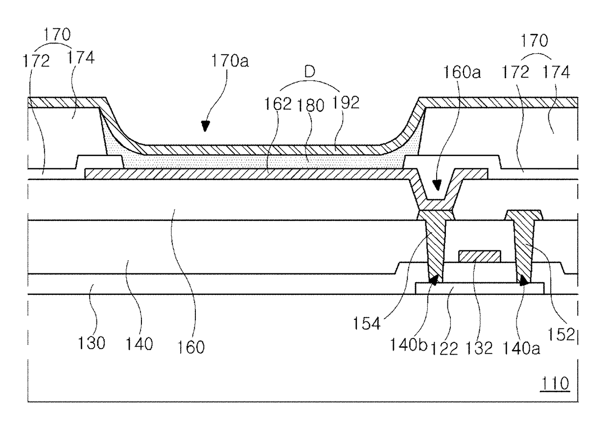
[0063]FIG. 4 is a cross-sectional view of an OLED display device according to a first embodiment of the present disclosure and shows one pixel region.
[0064]In FIG. 4, red, green, blue and white pixel regions Pr, Pg, Pb and Pw are defined on a substrate 110. The red, green, blue and white pixel regions Pr, Pg, Pb and Pw correspond to red, green, blue and white sub pixels, respectively, and the red, green, blue and white sub pixels constitute a pixel. A light emitting diode D is disposed in each pixel region Pr, Pg, Pb and Pw. The light emitting diode D includes a first electrode 162, a light emitting layer 180 and a second electrode 192. The light emitting layer 180 includes a hole injecting layer (HIL) 182, a hole transporting layer (HTL) 184, a light emitting material layer 186, and an electron transporting layer (ETL) 188.
[0065]More particularly, the first electrode 162 is formed in each of the red, green, blue and white pixel regions Pr, Pg, Pb and Pw as an anode. In the figure, ...
second embodiment
[0091]In a second embodiment of the present disclosure, a first light emitting material layer is formed in a white pixel region, and thus performance of a device can be improved.
[0092]FIG. 6 is a cross-sectional view of an OLED display device according to a second embodiment of the present disclosure and shows one pixel region.
[0093]In FIG. 6, red, green, blue and white pixel regions Pr, Pg, Pb and Pw are defined on a substrate 210. The red, green, blue and white pixel regions Pr, Pg, Pb and Pw correspond to red, green, blue and white sub pixels, respectively, and the red, green, blue and white sub pixels constitute a pixel. A light emitting diode D is disposed in each pixel region Pr, Pg, Pb and Pw. The light emitting diode D includes a first electrode 262, a light emitting layer 280 and a second electrode 292. The light emitting layer 280 includes a hole injecting layer (HIL) 282, a hole transporting layer (HTL) 284, a light emitting material layer 286, and an electron transportin...
PUM
Abstract
An organic light emitting diode includes a first electrode; a hole auxiliary layer on the first electrode; a light emitting material layer on the hole auxiliary layer and emitting white light; an electron auxiliary layer on the light emitting material layer; and a second electrode on the electron auxiliary layer, wherein the light emitting material layer includes a first light emitting material layer, a second light emitting material layer and a third light emitting material layer sequentially layered, and wherein the first light emitting material layer includes an electron blocking material.
Description
CROSS-REFERENCE TO RELATED APPLICATION[0001]The present application claims priority from and the benefit under 35 U.S.C. § 119(a) of Korean Patent Application No. 10-2016-0150542 filed on Nov. 11, 2016, which is hereby incorporated by reference in its entirety.BACKGROUND OF THE INVENTIONField of the Disclosure[0002]The present disclosure relates to an organic light emitting diodedisplay device, and more particularly, to an organic light emitting diode and an organic light emitting diodedisplay device including the same, which is capable of lowering power consumption.Discussion of the Related Art[0003]Recently, flat panel displays have been widely developed and applied to various fields because of their thin profile, light weight, and low power consumption.[0004]Among the flat panel displays, organic light emitting diode (OLED) display devices, which may be referred to as organic electroluminescent display devices, emit light due to the radiative recombination of an exciton after f...
Claims
Application Information
Patent Timeline
Application Date:The date an application was filed.
Publication Date:The date a patent or application was officially published.
First Publication Date:The earliest publication date of a patent with the same application number.
Issue Date:Publication date of the patent grant document.
PCT Entry Date:The Entry date of PCT National Phase.
Estimated Expiry Date:The statutory expiry date of a patent right according to the Patent Law, and it is the longest term of protection that the patent right can achieve without the termination of the patent right due to other reasons(Term extension factor has been taken into account ).
Invalid Date:Actual expiry date is based on effective date or publication date of legal transaction data of invalid patent.

