Optical fingerprint recognition sensor package

Inactive Publication Date: 2018-05-24
TRON INTELLIGENCE
View PDF6 Cites 2 Cited by
  • Summary
  • Abstract
  • Description
  • Claims
  • Application Information

AI Technical Summary

Benefits of technology

The present invention provides an optical fingerprint recognition sensor package which effectively filters out ambient lights and miscellaneous lights from interfering with the image sensor, resulting in increased accuracy and precision of sensing and recognition results. This is achieved by using two different molding compounds, namely a first molding compound made of infrared material and a second molding compound made of colored silicone, which correspond to the image sensor and the light emitting diode, respectively. The first molding compound is adjacent to the image sensor and hinders ambient lights from interfering with it, while the second molding compound provides a lighting path for the light source. The usage of two molding compounds reduces miscellaneous interferences from the ambient lights and enhances the accuracy and precision of the sensing results.

Problems solved by technology

However, since the structure of the semiconductor type is usually much more complicated and requires high complexity when being manufactured, the optical type is advantageous and profitable instead.
However, so far as we know, this is not very effective.
And an even worse problem is, by disposing an existence of the blocking-bar element, it usually results in an uneven distribution of the emitted light source, thereby affecting the estimated consequence of the image sensor and accuracy of the sensing and recognition outcomes.

Method used


Image

  • Optical fingerprint recognition sensor package
  • Optical fingerprint recognition sensor package
  • Optical fingerprint recognition sensor package

Examples


first embodiment

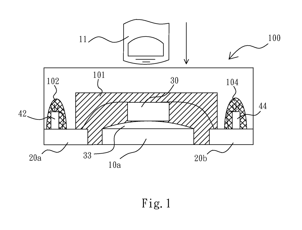
[0024]The present invention discloses an optical fingerprint recognition sensor package which can be utilized for eliminating interferences from the ambient lights and meanwhile increasing both the light sensing and recognition efficiency. Please refer to FIG. 1 first, which shows a cross sectional view of an optical fingerprint recognition sensor package in accordance with the present invention. As shown in FIG. 1, the optical fingerprint recognition sensor package 100 of the present invention comprises at least: a carrier, at least one image sensor 30, at least one light emitting diode 42,44, a first molding compound 101 and at least one second molding compound 102,104. According to one embodiment of the present invention, the carrier can be a substrate or alternatively a lead frame, and the carrier comprises a first part 10a and at least one second part 20a,20b for respectively disposing the above mentioned image sensor 30 and the light emitting diode 42,44. According to the embo...

second embodiment

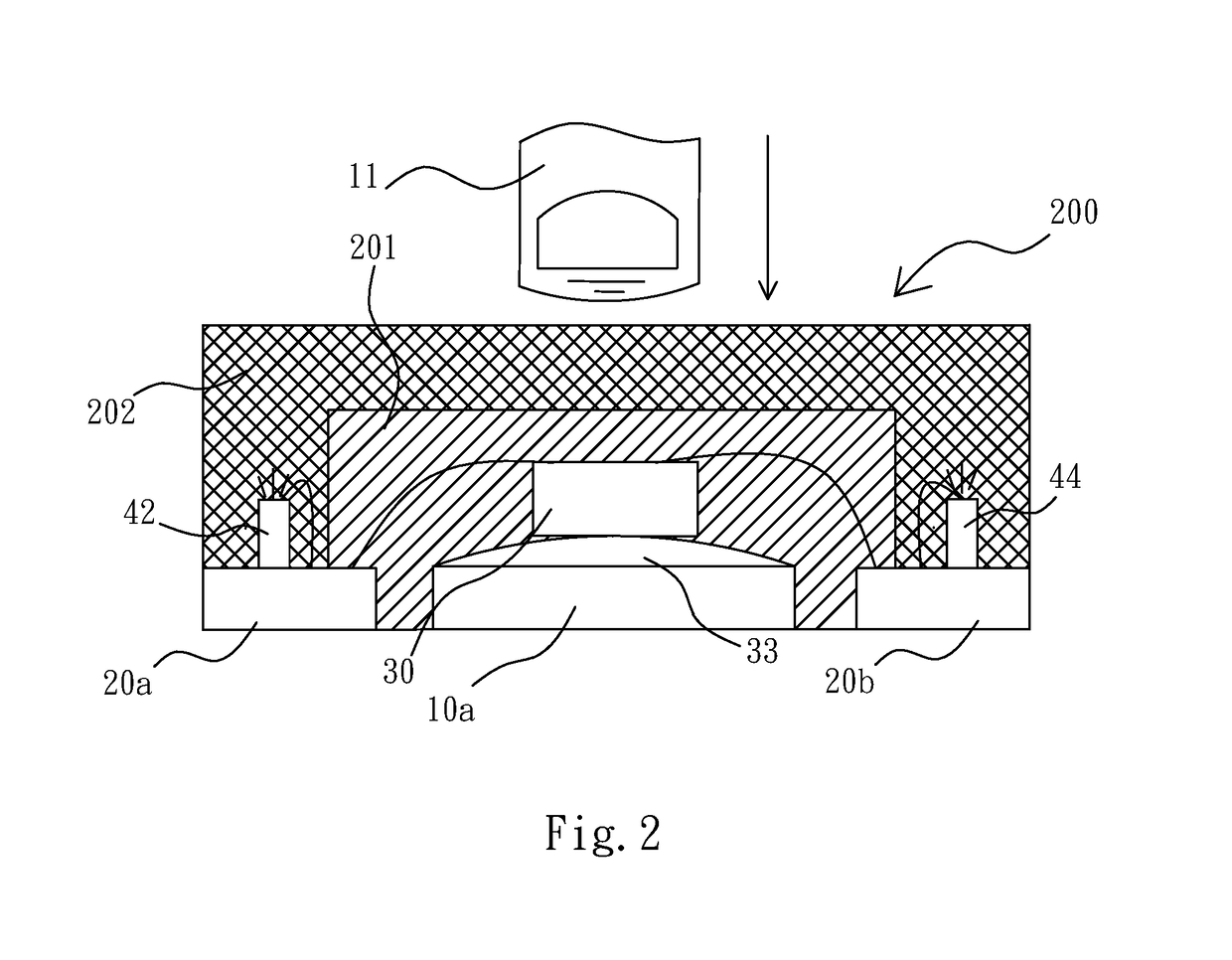
[0030]Next, please refer to FIG. 2, which shows a cross sectional view of an optical fingerprint recognition sensor package in accordance with the present invention. As shown in FIG. 2, the optical fingerprint recognition sensor package 200 of the present invention comprises at least: a carrier, at least one image sensor 30, at least one light emitting diode 42,44, a first molding compound 201 and at least one second molding compound 202. According to one embodiment of the present invention, the carrier is a substrate or alternatively a lead frame, and the carrier comprises a first part 10a and at least one second part 20a,20b for respectively disposing the above mentioned image sensor 30 and the light emitting diode 42,44. In one embodiment, the light emitting diode 42,44 is an infrared (IR) LED, being mounted on the second part 20a,20b of the carrier through an adhesive layer by surface-mount technology (SMT). In general, the adhesive layer for example can be a red glue or a silve...

third embodiment

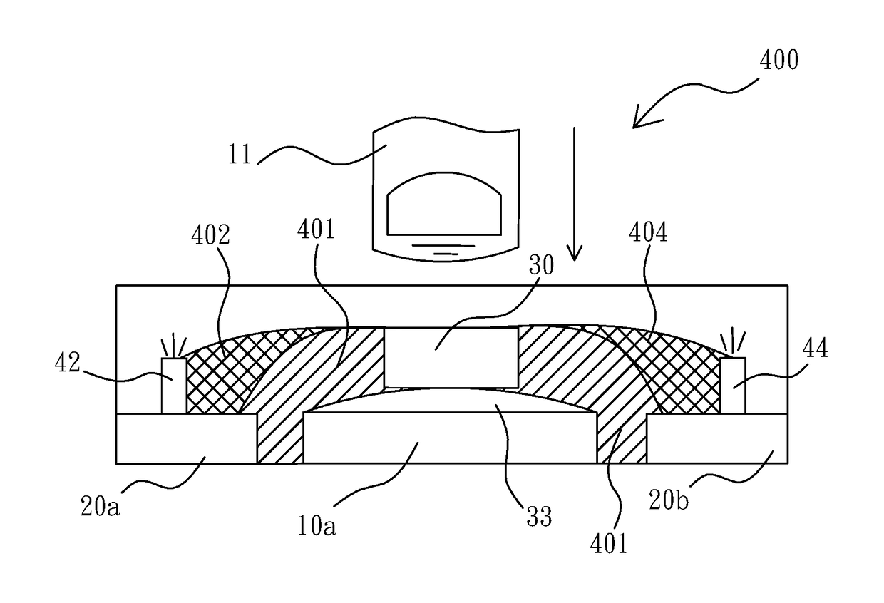
[0033]In addition, FIG. 3 shows a cross sectional view of an optical fingerprint recognition sensor package in accordance with the present invention. As shown in FIG. 3, the optical fingerprint recognition sensor package 300 of the present invention comprises at least: a carrier (10a, 20a, 20b), at least one image sensor 30, at least one light emitting diode 42,44, a first molding compound 301 and at least one second molding compound 302. The first part 10a of the carrier and at least one second part 20a,20b of the carrier are used for respectively disposing the above mentioned image sensor 30 and the light emitting diode 42,44. According to the embodiment of the present invention, the first part 10a of the carrier and the second part 20a,20b of the carrier are separated. The image sensor 30 is electrically connected with the second part 20a,20b of the carrier by conductive wire bonding, and each of the light emitting diode 42,44 is electrically connected with the second part 20a,20...


PUM


Abstract

An optical fingerprint recognition sensor package, which comprises a carrier, at least one image sensor, at least one light emitting diode, a first molding compound and at least one second molding compound is provided. The image sensor is disposed on the carrier and being electrically connected thereto. The at least one light emitting diode is peripherally surrounding the image sensor for providing at least one light source. The first molding compound made of infrared material is configured to be adjacent to the image sensor to hinder ambient lights from interfering with the image sensor. The second molding compound made of colored silicone is disposed over the light emitting diode to provide lighting path for the light source. By employing the proposed present invention, interferences from the ambient lights with the image sensor can be effectively avoided, thus increasing the accuracy and precision of the sensing results.

Description

REFERENCE TO RELATED APPLICATION[0001]This Patent Application is based on U.S. Provisional Patent Application Ser. No. 62 / 425,715, filed 23 Nov. 2016.BACKGROUND OF THE INVENTIONField of the Invention[0002]The present invention relates to an optical package structure, and more particularly to an optical fingerprint recognition sensor package.Description of the Prior Art[0003]Typically, the use of biometric data such as fingerprints in a security system, for example, portable communication devices (i.e. mobile phone, a tablet PC), financial transactions, home-based security and so on, may ensure efficient and accurate protection since fingerprints can be regarded as a certain kind of unique and standard manner of a person's distinctive identity verification. In general, fingerprints have a great number of features including ridges, valleys, and finer points, and a finer point includes a bifurcation where a ridge is branched and an end point where the ridge ends. Since one's fingerprin...

Claims


Application Information

Patent Timeline
IPC IPC(8): G06K9/00H01L31/167H01L25/16
CPCG06K9/00013H01L31/167H01L25/167H01L25/165H01L27/14618H01L27/14636H01L23/13H01L23/3107G06V40/12H01L27/14678H01L2924/18165H01L2924/15153H01L2224/48091H01L24/48H01L24/32H01L2224/32245H01L2224/48247H01L2224/48227H01L2224/32227H01L2224/48157H01L2224/48177H01L2224/49175H01L24/49H01L2224/29294H01L2224/29339H01L2224/2919H01L2224/83862H01L24/29H01L2924/12041H01L2924/00014G06V40/1318H01L2224/45099H01L24/16H01L2224/16245H05K1/181H05K2201/10106H05K2201/10151
Inventor TZU, DA-CHINGLIN, RUEY-JIANN
Owner TRON INTELLIGENCE
Why Eureka
Try Eureka