

Off-axis micro-mirror arrays for optical coupling in polymer waveguides
a polymer waveguide and micromirror array technology, applied in the field of micromirror arrays in waveguide arrays, can solve the problems of optical loss of several dbs and the problem becomes even more acu
- Summary
- Abstract
- Description
- Claims
- Application Information
AI Technical Summary
Benefits of technology
Problems solved by technology
Method used
Image

Examples
Embodiment Construction
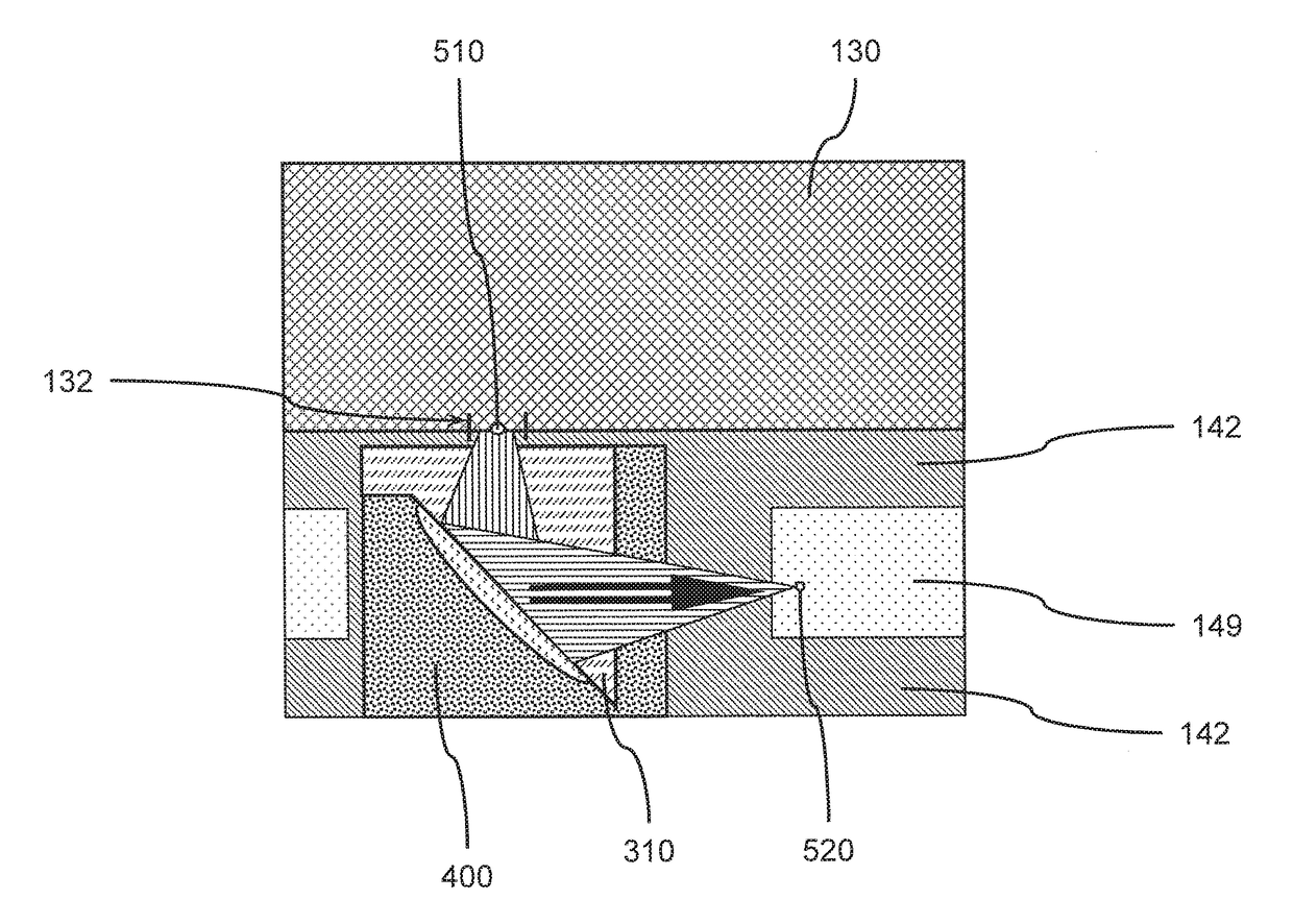
[0040]Principles and embodiments of the present invention relates generally to reducing optical losses incurred by coupling light signals through different transmission mediums in which the light signal propagates across multiple interfaces with different indexes of refraction and undergoes beam broadening that exacerbates light leakage at the interfaces and coupling junctions.
[0041]Principles and embodiments of the present invention also relate to an approach that reduces the current optical loss of several dBs by more efficiently coupling light beams to waveguides and photo-devices, particularly where an important cause of this loss is that the far-field profile of light emitted by a VCSEL at the output of a waveguide is too large, so that optical coupling is not efficient. Similarly, the far field profile at the end of a waveguide can be too large, so that optical coupling to a photodiode or fiber connector is not efficient.
[0042]Principles and embodiments of the present inventio...
PUM
 Abstract
Description
Claims
Application Information