Memory control circuit and method thereof

a memory control circuit and memory technology, applied in the field of memory control circuits, can solve the problems of increasing circuit area and manufacturing costs of socs, increasing the cost of socs, etc., and achieves simple and flexible circuits, enhancing the stability of read operations of spi nor flash memory

Active Publication Date: 2018-05-31
REALTEK SEMICON CORP
View PDF0 Cites 1 Cited by
  • Summary
  • Abstract
  • Description
  • Claims
  • Application Information

AI Technical Summary

Benefits of technology

[0007]The memory control circuit and method of the present invention are capable of adaptively determining a delay time period to compensate the signal delay caused by a routing on the circuit board and/or an in-chip routing. Compared to c

Problems solved by technology

However, the intermediary circuit 32 may result in additional costs su

Method used


Image

  • Memory control circuit and method thereof
  • Memory control circuit and method thereof
  • Memory control circuit and method thereof

Examples


Embodiment Construction

[0016]The following description is written by referring to terms of this technical field. If any term is defined in this specification, such term should be explained accordingly. In addition, the connection between objects or events in the below-described embodiments can be direct or indirect provided that these embodiments are practicable under such connection. Said “indirect” means that an intermediate object or a physical space exists between the objects, or an intermediate event or a time interval exists between the events.

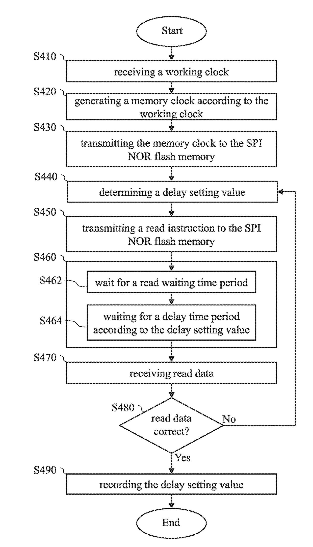
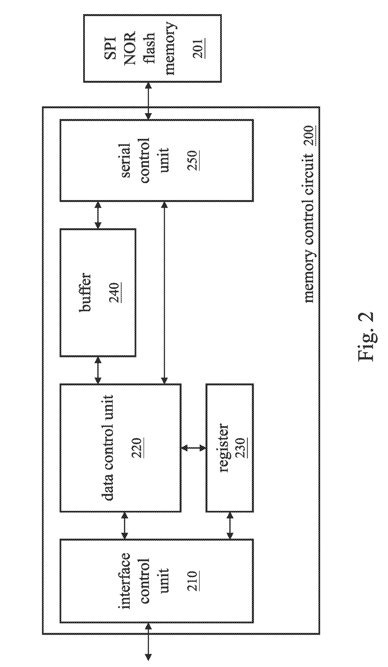
[0017]FIG. 2 shows a function block diagram of a memory control circuit according to an embodiment of the present invention. Referring to FIG. 2, a memory control circuit 200 is capable of performing a correction process and a normal operation process. FIG. 3 is a timing diagram of a read operation corresponding to FIG. 2. FIG. 4 shows a flowchart of a correction process of a memory control method according to an embodiment of the present invention. The memory...


PUM


Abstract

This invention discloses a memory control circuit and a method thereof. The memory control method includes the steps of: transmitting a first clock to a serial peripheral interface (SPI) NOR flash memory; transmitting a read instruction to the SPI NOR flash memory; waiting for a read waiting time period, which is associated with a specification of the SPI NOR flash memory and a cycle of the first clock; waiting for a delay time period, which is associated with a delay setting value and a cycle of a second clock different from the first clock; receiving read data returned from the SPI NOR flash memory; and adjusting the delay time period according to whether the read data are correct or not. This invention improves the stability of read operation of the SPI NOR flash memory and has advantages of simple circuit and flexible adjustment.

Description

BACKGROUND OF THE INVENTION1. Field of the Invention[0001]The present invention relates to a memory control circuit, especially to a control circuit and method for a serial peripheral interface (SPI) NOR flash memory.2. Description of Related Art[0002]FIG. 1 shows a schematic diagram of an application circuit of a conventional serial peripheral interface (SPI) NOR flash memory. A system-on-chip (SoC) 30 and an SPI NOR flash memory 20 are disposed on a circuit board 10. The SoC 30 uses a memory control circuit 31 to access data of the SPI NOR flash memory 20. Due to possible data delay caused by a routing 41 between the SoC 30 and the SPI NOR flash memory 20, the SoC 30 further includes an intermediary circuit 32 for solving an issue of asynchronous data that is caused by the routing 41 on the circuit board 10. Thus, only data delay caused by an in-chip routing 42 needs to be considered in the design of the SoC 30. However, the intermediary circuit 32 may result in additional costs s...

Claims


Application Information

Patent Timeline
IPC IPC(8): G11C16/26G06F13/14G06F13/42G11C16/32G11C8/06
CPCG11C16/26G06F13/14G06F13/4282G11C16/32G11C8/06G11C7/222G11C7/225G11C29/023G11C29/028
Inventor CHANG, YA-MIN
Owner REALTEK SEMICON CORP
Why Eureka
Try Eureka