Quality inspection of thin film materials

a thin film material and quality inspection technology, applied in resistance/reactance/impedence, material analysis, instruments, etc., can solve the problems of large-scale conductivity measurement, time-consuming raster scan across the sample, low reliability and spatial resolution of measurement techniques, etc., to achieve convenient alignment of the thin film material structure, less time-consuming, compact device design

Active Publication Date: 2018-06-14
ASSOC CENT DE INVESTIGACION COOP & NANOCIENCIAS CIC NANOGUNE +2
View PDF3 Cites 5 Cited by
  • Summary
  • Abstract
  • Description
  • Claims
  • Application Information

AI Technical Summary

Benefits of technology

[0012]In some examples, the conductivity may be determined at a single point of the thin-film samples. In other examples, raster scanning may be performed in order to calculate the conductivity at the adjacent points of the thin-film sample in order to obtain a large-area map of THz conductivity within the entire thin film material sample. The large-area map of THz conductivity, in turn, provides a quality metric where the effect of several physical features of the material, such as defects (e.g holes or multilayer points) and variations in doping density, is reflected. Additionally or alternatively other parameters may be calculated to create the map and assess the quality of the material.
[0013]The present invention demonstrates an advantage compared to other solutions for obtaining the THz conductivity of the material disclosed in the literature where the transmission configuration is used and, thus, the access to the bottom side of the sample is required. The solution given in the present invention is based on the measurement using a reflection configuration and thus allows the positioning of both the THz source emitter and the THz detector at the same side of the sample under test. This aspect of the invention is fundamental for its practical application in industry as a quality inspection tool.
[0014]Another advantage of using the THz radiation for quality inspection of the thin film material is the fact that it is a non-contact method and, thus, it does not require ohmic contacts, which may affect measurement results and lead to damages in the surface of the sample. At the same time, it bridges the gap between nano / micro scale tools and macro, whole-sample scale tools. Therefore, the method is less time-consuming and it offers an efficient alternative for the electrical characterization of small-scale and large-scale samples of thin film materials. Note that, the term of small-scale refers to the samples that have the area of less than 10 cm2, while the large-scale sample has an area of at least 10 cm2 or larger. In some embodiment, large-scale samples are linked together to create structures that include multiple large-scale samples.
[0015]In some examples, the THz source emitter and the THz detector are incorporated in a single THz source / detector module and wherein the irradiation and reflection directions coincide. This allows for a compact design of the device and easier alignment of the thin film material structure.
[0016]In some examples, several THz sources / detectors modules or an array of THz modules may be used in order to improve the speed of the measuring system.
[0017]In other examples, the THz source emitter and the THz detector are spaced apart and wherein the incidence of the irradiation is oblique with an angle of incidence α. This allows for the easier separation of the emitted and received signal thus avoiding interferences.

Problems solved by technology

The small-scale and large-scale measurement of the conductivity is an important issue in the non-contact quality inspection of thin film materials.
This measurement technique is characterized by its low reliability and spatial resolution as it provides a single value of DC conductivity of the whole sample (see “Graphene Conductance Uniformity Mapping”, Buron et al., Nanoletters, 12 (10), pp 5074-50812012).
Thus, in order to characterize the material, the time-consuming raster scan needs to be performed across the entire sample.
Consequently, Raman spectroscopy is not an adequate method to characterize large-scale samples (≥10 cm2).
Moreover, it does not provide any quantitative information about the distribution of the conductivity in the sample.
Moreover, the usage of this measurement technique may lead in some cases to damages in the material under test.
Several examples included in the literature present the methods to calculate the conductivity of thin film materials using the transmission configuration, which is often not appropriate in an industrial process as it requires placing the radiation emitter and detector at the opposite sides of the measured material.

Method used


Image

  • Quality inspection of thin film materials
  • Quality inspection of thin film materials
  • Quality inspection of thin film materials

Examples


Embodiment Construction

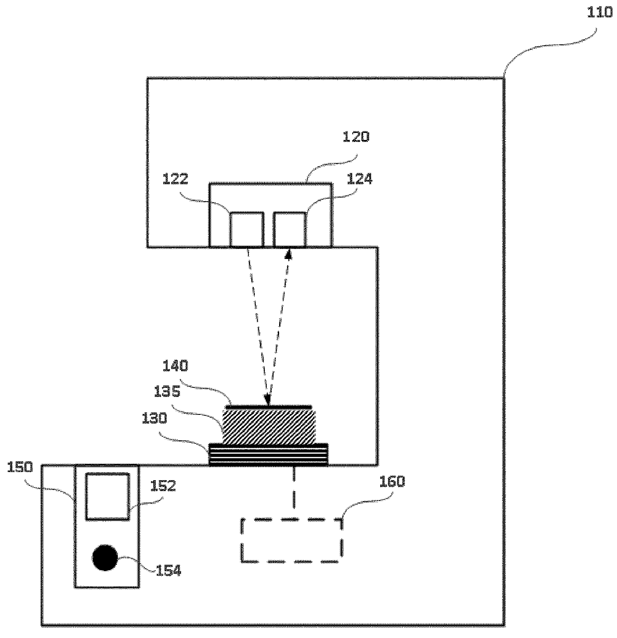
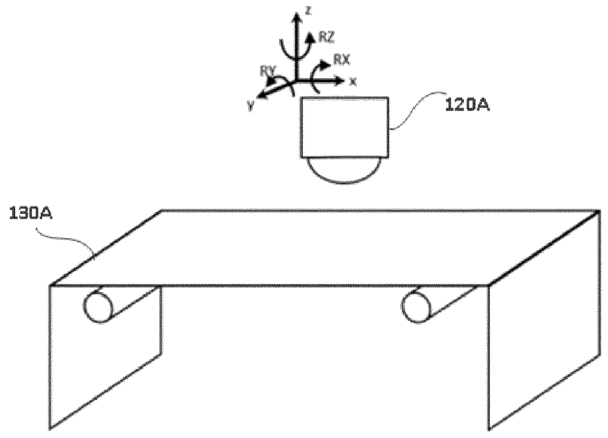
[0067]FIG. 1B illustrates a device to determine the quality of a thin film material according to an example. Device 100 may comprise a housing 110, a THz module 120 and a reflective base 130. The THz module 120 may comprise a THz source emitter 122 and a THz detector 124. A thin film material 140 is illustrated on top of a substrate 135. An actuator 160 may selectively move the reflective base 130 to change the distance between the THz source emitter 122 and the surface of the thin film material 140 as well as the point of incidence of the irradiation.

[0068]During a sample inspection process, the sample 140 to be measured is placed on the reflective base 130, to maximize the reflection of the signal. The reflective base 130 may be a metallic base. However, other materials with a high conductivity, i.e. materials with high reflectivity in the THz frequency range, such as semiconductor materials (e.g. doped silicon or similar) may be used as materials for the reflective base 130. Now,...


PUM

PropertyMeasurementUnit
areaaaaaaaaaaa
areaaaaaaaaaaa
areaaaaaaaaaaa

Abstract

Devices and methods for determining the quality thin film materials are disclosed. The thin film materials are provided on substrates forming thin film material structures. The devices comprise a housing, a THz module with a THz source emitter and a THz detector,and a reflective base moveable relative to the THz module and configured to support the thin film material structures. The THz source emitter is configured to irradiate the thin film materials. The THz detector is configured to measure at least one reflection of the irradiation. The device is configured to calculate a parameter indicative of the quality of the thin film material based on said reflection measurements.

Description

[0001]The present disclosure relates to thin film materials and more specifically to devices and methods for evaluating the quality of thin film materials by measuring their conductivity.BACKGROUND ART[0002]Thin film materials made of thin sheets of atoms are novel structures characterized by unique specifications that can be used to improve electrical, mechanical, thermal, and optical properties of other materials. Graphene is an example of such atomically thin materials with many commercial applications, either proposed and / or under development in a variety of technical areas. The behavior of transmitted and reflected electromagnetic waves when they interact with thin film materials depends on several properties, most importantly, on their sheet conductivity, in such a way that areas of higher sheet conductivity are characterized by higher reflectivity and areas of higher transmittance are related with lower sheet conductivity of this material. The conductivity of the material and...

Claims


Application Information

Patent Timeline
Patent Type & Authority Applications(United States)
IPC IPC(8): G01R27/02G01N21/84
CPCG01R27/02G01N21/84G01N2021/178G01N21/3581G01N21/8422G01N21/55G01N21/59
Inventor AZANZA LADRON, EDUARDOCHUDZIK, MAGDALENALOPEZ ZORZANO, ALEXETAYO SALINAS, DAVIDHUESO ARROYO, LUIS EDUARDOZURUTUZA ELORZA, AMAIA
Owner ASSOC CENT DE INVESTIGACION COOP & NANOCIENCIAS CIC NANOGUNE
Why Eureka
Try Eureka