Light emitting diode chip

a technology of light-emitting diodes and diodes, which is applied in the direction of basic electric elements, electrical equipment, semiconductor devices, etc., can solve the problems of inferior efficiency of led chips, and achieve the effects of good performance, thin thickness, and small area

Active Publication Date: 2018-06-14
PLAYNITRIDE
View PDF4 Cites 4 Cited by
  • Summary
  • Abstract
  • Description
  • Claims
  • Application Information

AI Technical Summary

Benefits of technology

[0005]The disclosure provides a light emitting diode (LED) chip having good performance with smaller area and thinner thickness.

Problems solved by technology

However, when the area of μLED chip is reduced (e.g. at the level of a plurality of square microns), the electron and hole in the μLED chip are easily transmitted to a side wall of the μLED chip and combined in the defect of the side wall with no emission of light, which is not preferable for the light-emitting property of the μLED chip.
Besides, an originally overly-thick semiconductor layer is likely to absorb light due to minimization of the size of μLED chip, causing the efficiency of the μLED chip to become inferior.

Method used


Image

  • Light emitting diode chip
  • Light emitting diode chip
  • Light emitting diode chip

Examples


Embodiment Construction

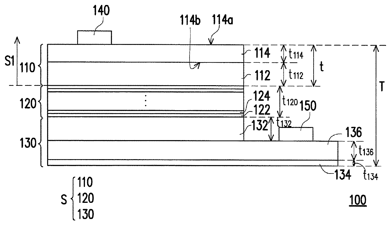
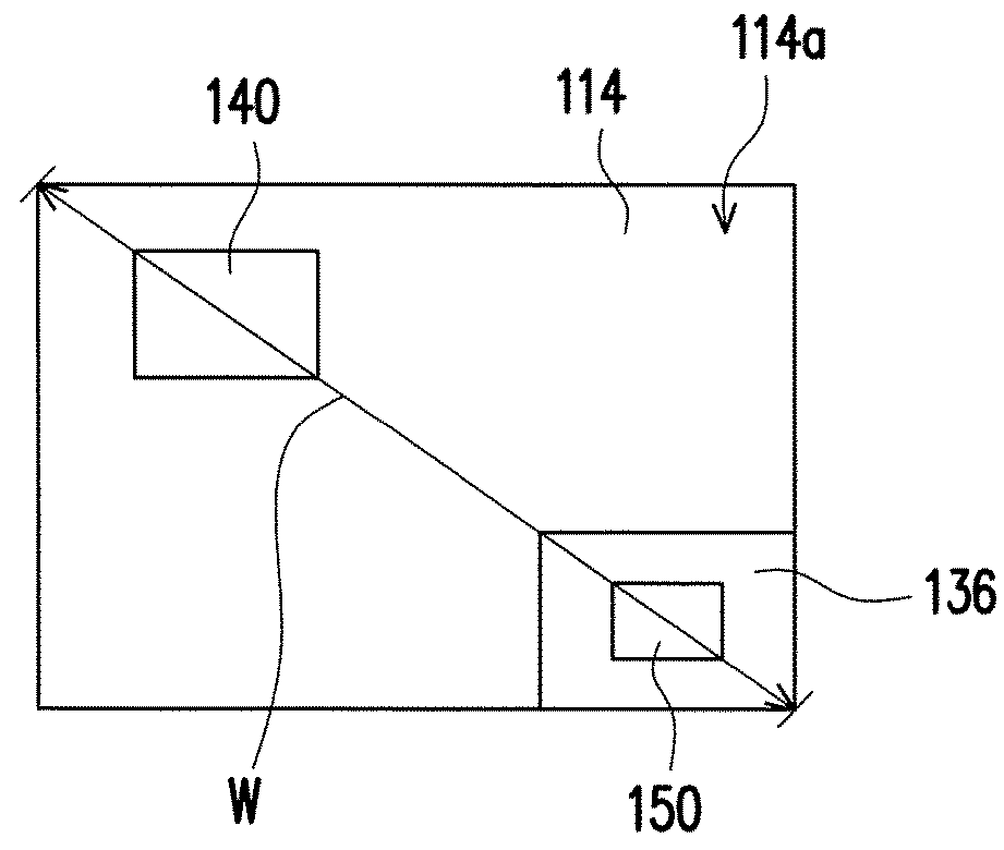
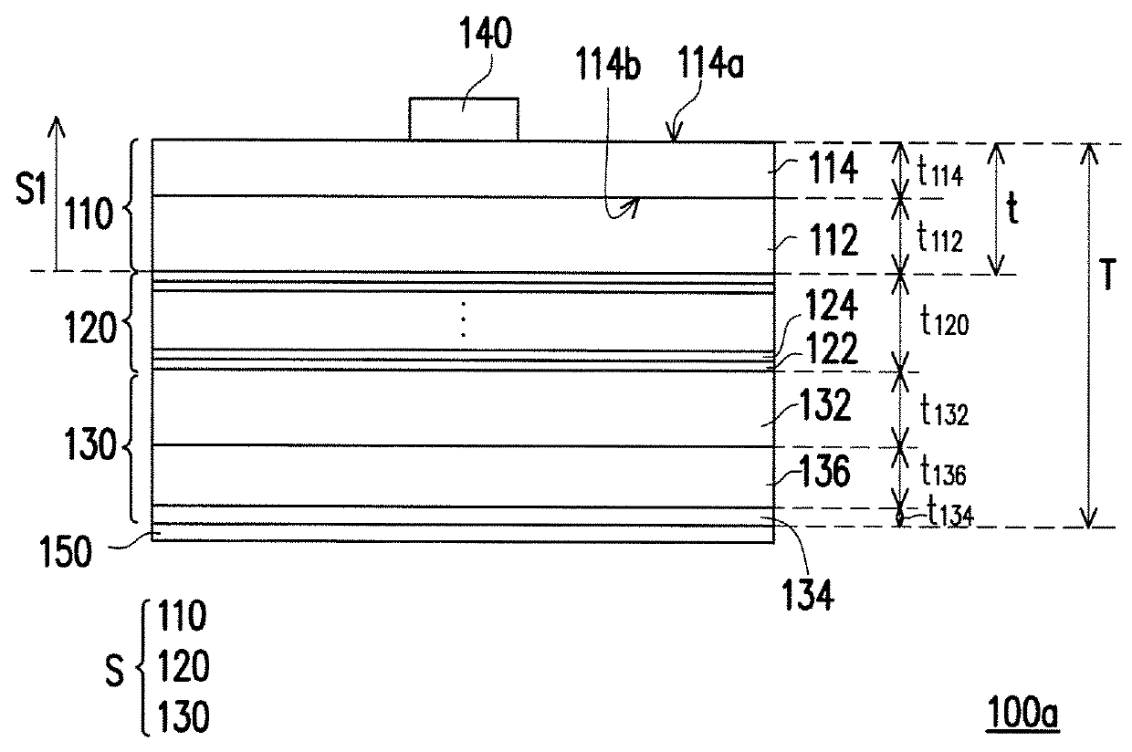
[0022]FIG. 1A is a sectional view of a light emitting diode (LED) chip according one embodiment of the disclosure. FIG. 1B is a top view of the LED chip in FIG. 1A. Referring to FIGS. 1A and 1B, an LED chip 100 comprises a p-type semiconductor layer 110, a light-emitting layer 120 and an n-type semiconductor layer 130. The light-emitting layer 120 is disposed between the p-type semiconductor layer 110 and n-type semiconductor layer 130. In the embodiment, the light-emitting layer 120 is configured to emit red light. In other words, the LED chip 100 is a red-light LED chip.

[0023]In the embodiment, the light-emitting layer 120 may be a multiple quantum well structure. Specifically, the light-emitting layer 120 comprises a plurality of barrier layers 122 and a plurality of well layers 124 alternately stacked on each other, wherein an energy gap of the barrier layer 122 is larger than the energy gap of the well layer 124. In the embodiment, the material of the barrier layer 122 and the ...


PUM


Abstract

A light-emitting diode chip including a p-type semiconductor layer, a light-emitting layer and an n-type semiconductor layer is provided. The light-emitting layer is disposed between the p-type semiconductor layer and the n-type semiconductor layer. A ratio of a sum of thicknesses of all semiconductor layers of the light-emitting diode chip over a maximum width of the light-emitting diode chip ranges from 0.02 to 1.5. A ratio of a sum of thicknesses of all semiconductor layers located in a side of the light-emitting layer toward the p-type semiconductor layer over the sum of thicknesses of all semiconductor layers of the light-emitting diode chip ranges from 0.05 to 0.2.

Description

CROSS-REFERENCE TO RELATED APPLICATION[0001]This application claims the priority benefit of Taiwan application serial no. 105140653, filed on Dec. 8, 2016. The entirety of the above-mentioned patent application is hereby incorporated by reference herein and made a part of this specification.BACKGROUND OF THE DISCLOSUREField of the Disclosure[0002]The disclosure relates to a light emitting element, and particularly to a light emitting diode chip.Description of Related Art[0003]Micro light emitting diode (μLED) display includes a display substrate and a plurality of μLED chips electrically connected with the display substrate. Each pixel region of the μLED display is provided with a corresponding μLED chip, and each μLED chip can emit light independently. With the characteristic of LED, the μLED display has the advantages of being low-power consumption, high brightness, color saturation, fast respond speed, power-saving, etc. In addition, the μLED display is superior with good materia...

Claims


Application Information

Patent Timeline
Patent Type & Authority Applications(United States)
IPC IPC(8): H01L33/20H01L33/06H01L33/30
CPCH01L33/20H01L33/06H01L33/42H01L33/405H01L33/30
Inventor WU, JYUN-DELO, YU-YUN
Owner PLAYNITRIDE
Why Eureka
Try Eureka