Array substrate, display device and manufacturing method for array substrate

Active Publication Date: 2018-06-21
WUHAN CHINA STAR OPTOELECTRONICS TECH CO LTD
View PDF5 Cites 2 Cited by
  • Summary
  • Abstract
  • Description
  • Claims
  • Application Information

AI Technical Summary

Benefits of technology

[0025]In the present embodiment, because in the array substrate, the isolation layer is disposed between the array substrate and the buffering layer, and the isolation layer adopts a metal material, in the process of manufacturing the buffering layer through a high-temperature Plasma Enhanced Chemical Vapor Deposition (PECVD), the isolation layer can prevent an organic m

Problems solved by technology

Because water isolation, oxygen barrier, and heat resistance abilities of the organic material substrate are poor, and when manufacturing a Low temperature poly-silicon (LTPS) flexible display device, a high-temperature process such as the Eximer laser annealing (ELA) is required.
The buffering layer deposited through

Method used


Image

  • Array substrate, display device and manufacturing method for array substrate
  • Array substrate, display device and manufacturing method for array substrate
  • Array substrate, display device and manufacturing method for array substrate

Examples


Embodiment Construction

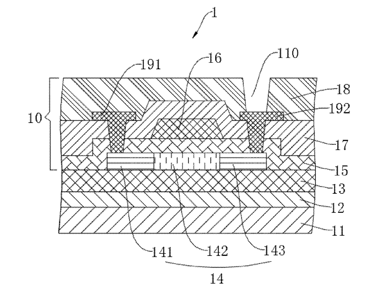
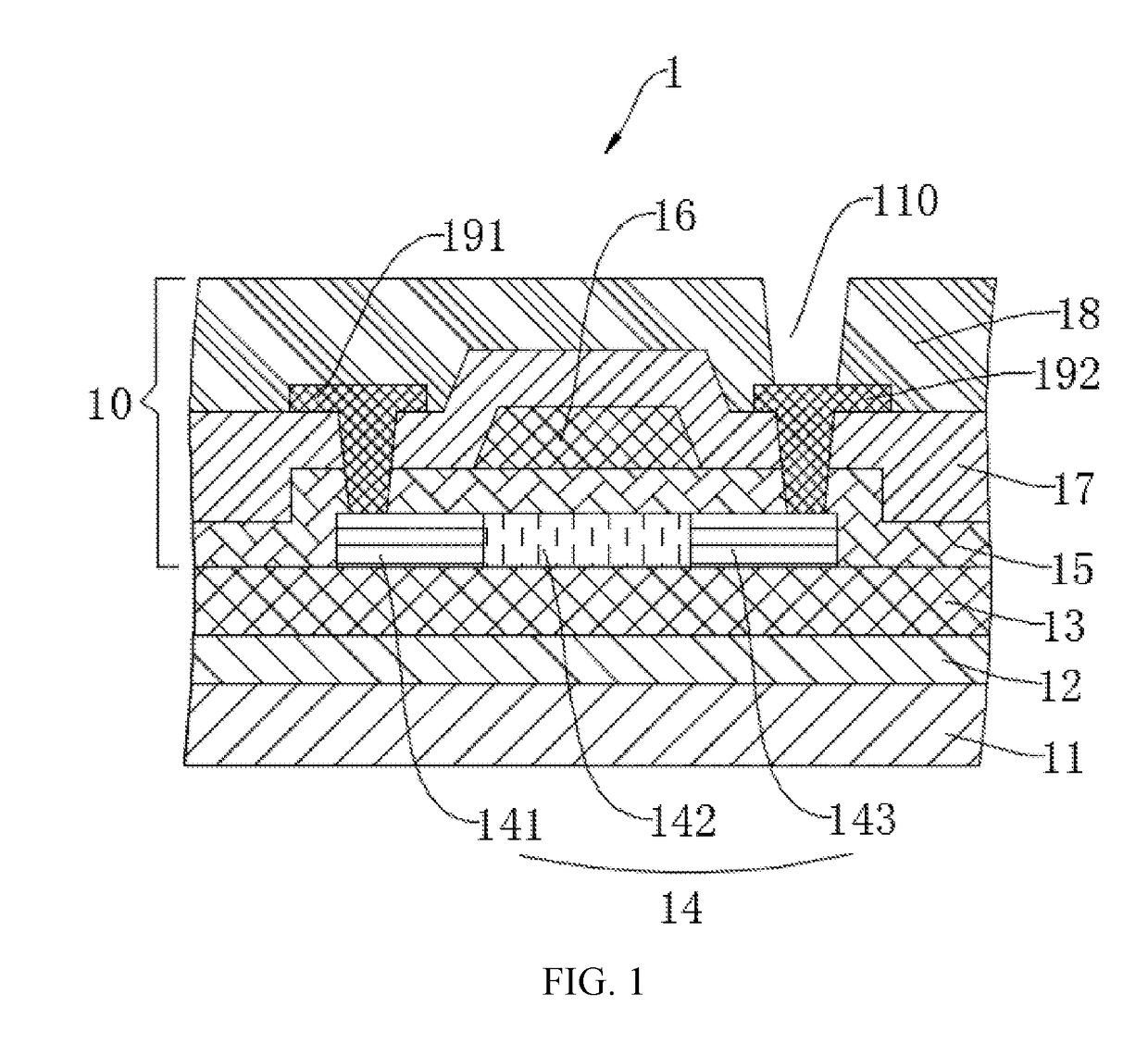
[0030]The following content combines with the drawings and the embodiment for describing the present invention in detail. It is obvious that the following embodiments are only some embodiments of the present invention. For the person of ordinary skill in the art without creative effort, the other embodiments obtained thereby are still covered by the present invention.

[0031]Besides, the description of the following embodiments is referred to the appended figures in order to exemplarily illustrate the specific embodiments of the present invention. The directional terms mentioned in the present invention such as “up”, “down”, “front”, “rear”, “left”, “right”, “inside”, “outside”, “side surface” and so on only refer to the direction of appended figures. Therefore, the adopted directional terms are for describing and understanding the present invention better and more clearly, not for indicating or implying the device or component having specific direction or operating by using a specifi...


PUM


Abstract

An array substrate is disclosed. The array substrate includes: a substrate adopting an organic material; an isolation layer adopting a metal material, and the isolation layer is formed on the substrate; and a buffering layer formed at a side of the isolation layer away from the substrate. In the array substrate of the present invention, in a high-temperature PECVD process, a pollution problem caused by the plasma directly bombarding the substrate made of an organic material can be avoid. A display device applying the array substrate and a manufacturing method for an array substrate are also disclosed.

Description

CROSS REFERENCE[0001]The claims of this application have submitted to the State Intellectual Property Office of the People's Republic of China (SIPO) on May 31, 2016, Application No. 201610375303.0. The priority right based on the China application has a title of “Array substrate, display device and manufacturing method for array substrate”. The entire contents of the above-mentioned patent application will be incorporated in the present application through citing.FIELD OF THE INVENTION[0002]The present invention relates to a flexible display technology field, and more particularly to an array substrate, a display device and a manufacturing method for an array substrate.BACKGROUND OF THE INVENTION[0003]The conventional flexible display device is based on an organic material substrate. Because water isolation, oxygen barrier, and heat resistance abilities of the organic material substrate are poor, and when manufacturing a Low temperature poly-silicon (LTPS) flexible display device, ...

Claims


Application Information

Patent Timeline
IPC IPC(8): H01L27/12H01L27/32
CPCH01L27/1262H01L27/1218H01L27/3258H01L2227/323H10K59/12H01L29/78603H01L29/78675Y02P70/50H10K59/1213H10K77/111H10K50/844Y02E10/549H10K59/124H10K59/00H10K59/1201H01L21/84H01L27/12
Inventor QIN, FANG
Owner WUHAN CHINA STAR OPTOELECTRONICS TECH CO LTD
Why Eureka
Try Eureka