Massively parallel transfer of microLED devices

Inactive Publication Date: 2018-07-05
KUMAR ANANDA H +2
View PDF9 Cites 33 Cited by
  • Summary
  • Abstract
  • Description
  • Claims
  • Application Information

AI Technical Summary

Benefits of technology

[0005]In some embodiments, the present invention discloses methods to form microLED displays using a massively assembling process for connecting microLED devices onto a circuit substrate. The microLED devices can be transferred in large numbers to form microLED displays using processes such as pick-and-place, thermal adhesion transfer, or fluidic t

Problems solved by technology

However, the requirement for transfer and assembly (including terminal soldering and device alignments) is still re

Method used


Image

  • Massively parallel transfer of microLED devices
  • Massively parallel transfer of microLED devices
  • Massively parallel transfer of microLED devices

Examples


first embodiment

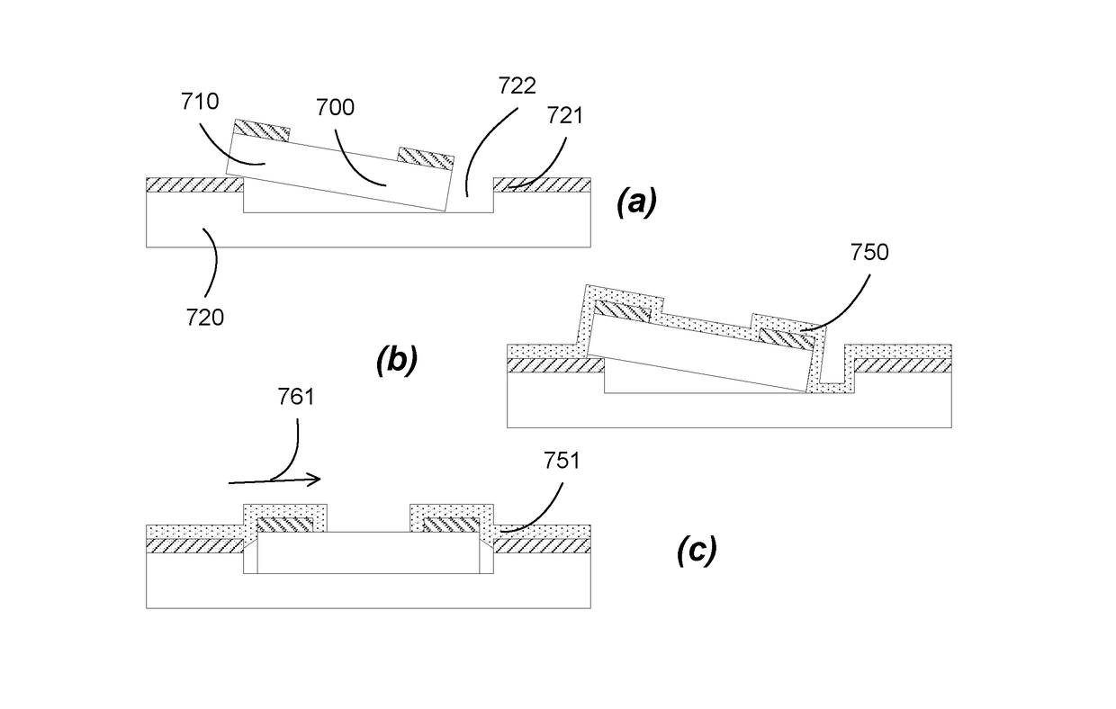
[0067]For the first embodiment, the microLED devices need to be oriented with their bond pads all pointing downwards, facing the terminal pads on the circuit board. When the devices are placed with the bond pads oriented downwards, they are in a flip chip attachment in approximate alignment with corresponding terminal pads of the board. The solder layer can be first placed on the circuit board, followed by the microLED devices on the solder layer with the bond pads contacting the solder layer. When the solder reflows, it will melt and coat the copper terminal pads and the nickel bond pads, simultaneously aligning them with each other, because of the surface tension of the solder.

second embodiment

[0068]In the second embodiment, the microLED devices can be oriented with their bond pads pointed upwards. The solder layer can be provided after the microLED devices are placed on the circuit board. Once the microLED devices are properly positioned with this upward orientation, the thin film of solder is formed on the circuit board. When the solder is melted, it can reach up to the nickel bond pads to complete the interconnection between the bond pads and the terminal pads.

[0069]In both cases, the solder wets the circuits and also de-wets from the bare areas of the circuit board (where there are no contact pads) which can easily be removed. For example, the excess solder can balls up and can be removed with air, water or ultrasound.

[0070]In some embodiments, the methods uses wave soldering process with a thin film of solder instead of a solder bath. The technique of Wave Soldering uses a molten solder bath. A circuit board is passed, upside down, on top of the molten solder, so tha...


PUM


Abstract

MicroLED devices can be transferred in large numbers to form microLED displays using processes such as pick-and-place, thermal adhesion transfer, or fluidic transfer. A blanket solder layer can be applied to connect the bond pads of the microLED devices to the terminal pads of a support substrate. After heating, the solder layer can connect the bond pads with the terminal pads in vicinity of each other. The heated solder layer can correct misalignments of the microLED devices due to the transfer process.

Description

[0001]The present application claims priority from the provisional application Ser. No. 62 / 429,877, filed on Dec. 5, 2016, which is hereby incorporated by reference in its entirety.[0002]MicroLED displays include multiple microLED devices assembled on a substrate having an interconnection networks for connecting bond pads of the microLED devices, e.g., to allow driver circuits to drive the microLED devices as individual pixels of the microLED displays.[0003]MicroLED devices are small, e.g., about 100 microns across. The assemblies for microLED displays require large numbers of the microLED devices in close-packed arrays.[0004]MicroLED displays can have large advantages, including low power consumption and high brightness. However, the requirement for transfer and assembly (including terminal soldering and device alignments) is still regarded after many years as a serious technological challenge blocking the commercial adoption of MicroLED displays.SUMMARY OF THE DESCRIPTION[0005]In ...

Claims


Application Information

Patent Timeline
IPC IPC(8): H01L23/00H01L33/62H01L25/075
CPCH01L24/83H01L33/62H01L25/0753H01L24/32H01L2933/0066H01L2224/83005H01L2224/32013H01L2224/32053H01L2224/3207H01L2224/32105H01L2224/32111H01L2224/32145H01L2224/32227H01L2224/83815H01L2224/83143H01L2224/83345H01L2224/83385H01L2224/8393H01L2924/12041H01L24/29H01L24/16H01L2224/16227H01L24/03H01L24/05H01L2224/05655H01L2224/0518H01L2224/2732H01L2224/2745H01L24/27H01L2224/29111H01L2224/291H01L2224/293H01L2224/29294H01L2224/29028H01L2224/82815H01L24/82H01L24/24H01L2224/24227H01L2224/82143H01L2224/82104H01L2924/15153H01L2224/82399H01L2224/97H01L24/97H01L2224/29006H01L2224/83192H01L2224/32237H01L2924/15157H01L2924/10156H01L2224/245H01L2224/83912H01L2224/82005H01L2224/82105H01L24/95H01L2224/95136H01L2224/95101H01L2224/95144H01L2224/75754H01L2224/76754H01L2224/83907H01L2224/83024H01L2224/83455H01L2224/81191H01L24/81H01L24/13H01L2224/81815H01L2224/81907H01L2224/81143H01L2224/81024H01L2224/8191H01L24/98H01L2224/8291H01L2224/8391H01L2224/8121H01L2224/82101H01L2224/82132H01L2224/83132H01L2224/05073H01L2224/03848H01L2224/131H01L24/75H01L24/76H01L2924/3841H01L2924/00012H01L2924/00014H01L2924/014H01L2924/01029H01L2224/82H01L2924/0105H01L2924/01028H01L2224/83H01L2224/81
Inventor KUMAR, ANANDA H.KUMAR, SRINIVAS H.NGUYEN, TUE
Owner KUMAR ANANDA H
Why Eureka
Try Eureka