Etching platinum-containing thin film using protective cap layer

a technology of protective cap layer and platinum-containing metal, which is applied in the direction of semiconductor/solid-state device details, chemistry apparatus and processes, transistors, etc., can solve the problems of difficult etching of platinum-containing metal, non-uniform wet etching, and platinum residue in the etched area

Active Publication Date: 2018-07-19
TEXAS INSTR INC
View PDF6 Cites 5 Cited by
  • Summary
  • Abstract
  • Description
  • Claims
  • Application Information

AI Technical Summary

Benefits of technology

This patent describes a method for making a microelectronic device by forming a layer of platinum on a substrate and adding a cap layer over the platinum layer. The cap layer is etchable in a solution that also removes the platinum layer. A hard mask can be used to pattern the platinum layer, and a subsequent wet etch process can remove the cap layer and the underlying platinum layer to create a patterned device. The technical effects of this method are better patterning and protection of the microelectronic device during etching.

Problems solved by technology

Etching platinum-containing metal is difficult.
Wet etching requires very strong acids such as aqua regia, and results in platinum-containing residue in the etched areas.
Moreover, wet etching tends to be non-uniform, requiring significant overetch, which introduces unwanted variation in lateral dimensions of the patterned layer.
Dry etching may be accomplished by sputter etching, also referred to as ion milling, but results in undesired redeposited platinum-containing material on the microelectronic device, which may reduce reliability of the microelectronic device.
Furthermore, sputter etching may result in depositing unwanted platinum containing residue on interior surfaces of the sputter etching chamber, which may cause contamination on subsequently processed wafers.
Sputter etching also has poor selectivity to materials in layers under the platinum-containing metal.

Method used


Image

  • Etching platinum-containing thin film using protective cap layer
  • Etching platinum-containing thin film using protective cap layer
  • Etching platinum-containing thin film using protective cap layer

Examples


Embodiment Construction

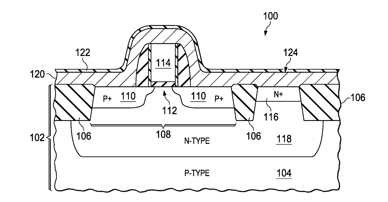
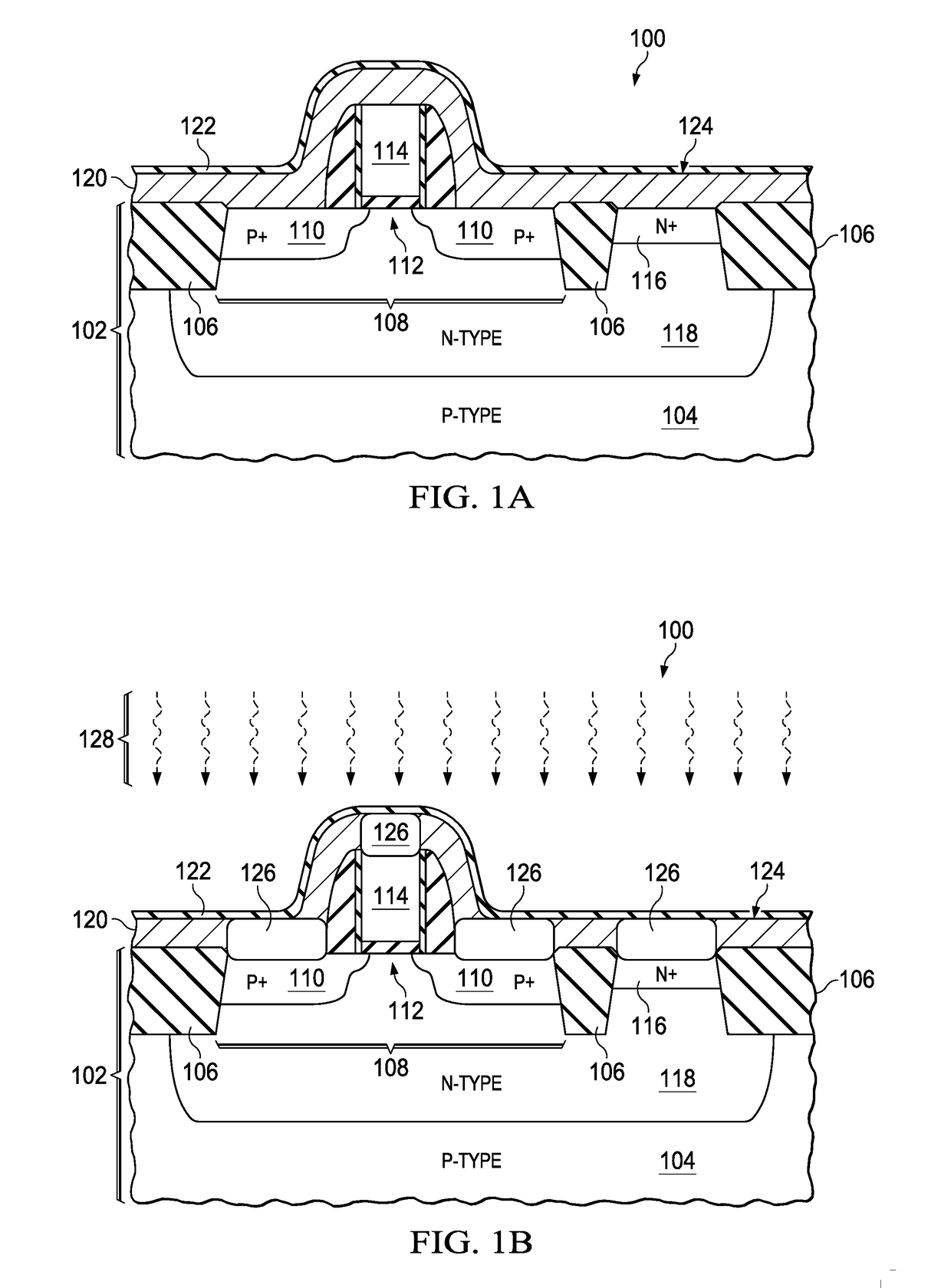
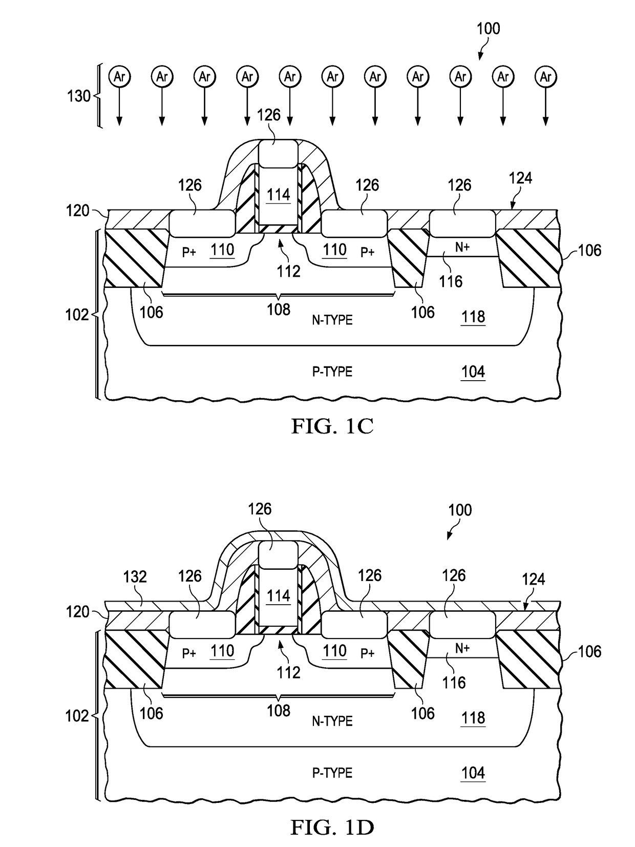
[0014]The present invention is described with reference to the attached figures. The figures are not drawn to scale and they are provided merely to illustrate the invention. Several aspects of the invention are described below with reference to example applications for illustration. It should be understood that numerous specific details, relationships, and methods are set forth to provide an understanding of the invention. The present invention is not limited by the illustrated ordering of acts or events, as some acts may occur in different orders and / or concurrently with other acts or events. Furthermore, not all illustrated acts or events are required to implement a methodology in accordance with the present invention.

[0015]A microelectronic device which includes a component having a platinum-containing layer may be formed by a method including forming the platinum-containing layer on an instant top surface of the microelectronic device. For the purposes of this disclosure, the te...


PUM


Abstract

A microelectronic device is formed by forming a platinum-containing layer on a substrate of the microelectronic device. A cap layer is formed on the platinum-containing layer so that an interface between the cap layer and the platinum-containing layer is free of platinum oxide. The cap layer is etchable in an etch solution which also etches the platinum-containing layer. The cap layer may be formed on the platinum-containing layer before platinum oxide forms on the platinum-containing layer. Alternatively, platinum oxide on the platinum-containing layer may be removed before forming the cap layer. The platinum-containing layer may be used to form platinum silicide. The platinum-containing layer may be patterned by forming a hard mask or masking platinum oxide on a portion of the top surface of the platinum-containing layer to block the wet etchant.

Description

CROSS-REFERENCE TO RELATED APPLICATIONS[0001]This application claims the benefit of priority under 35 U.S.C. §119(e) of U.S. Provisional Application No. 62 / 448,138 (Texas Instruments docket number TI-77675PS), filed Jan. 19, 2017, which is hereby incorporated by reference in its entirety.FIELD OF THE INVENTION[0002]This invention relates to the field of microelectronic devices. More particularly, this invention relates to metal layers in microelectronic devices.BACKGROUND OF THE INVENTION[0003]It may be desirable to form a patterned layer of platinum-containing metal in a microelectronic device. Etching platinum-containing metal is difficult. Wet etching requires very strong acids such as aqua regia, and results in platinum-containing residue in the etched areas. Moreover, wet etching tends to be non-uniform, requiring significant overetch, which introduces unwanted variation in lateral dimensions of the patterned layer. Dry etching may be accomplished by sputter etching, also refer...

Claims


Application Information

Patent Timeline
Patent Type & Authority Applications(United States)
IPC IPC(8): H01L21/311H01L21/263H10N97/00
CPCH01L21/31122H01L21/2633C01G55/004H01L23/53242H01L23/528H01L23/4827H01L23/485H01L21/02068H01L21/32134H01L21/32139C01G55/00H01L21/823814H01L21/823835H01L29/665H01L28/24H01L29/6659H01L29/7833H01L21/76885H01L21/76895H01L21/28518H01L21/76834H01L24/05H01L2224/04042H01L2224/03464H01L2224/05155H01L2224/05164H01L2224/05169H01L2224/05669H01L2224/05187H01L24/03H01L2224/0382H01L2224/03009H01L2224/85205H01L2224/45144H01L2224/45169H01L2224/48669H01L24/45H01L24/48H01L24/85H01L2224/13109H01L2224/11849H01L24/13H01L24/11H01L2224/85375H01L2224/03614H01L2224/0347H01L2224/03914H01L2924/00014H01L2924/054H01L2924/01078H01L2924/00012H01L29/4975H01L21/28052H01L24/00
Inventor MEIER, SEBASTIANRINCK, HELMUTMITTELSTAEDT, MIKE
Owner TEXAS INSTR INC
Why Eureka
Try Eureka