
Semiconductor device structure

Active Publication Date: 2018-07-19
GLOBALFOUNDRIES US INC
View PDF7 Cites 4 Cited by
  • Summary
  • Abstract
  • Description
  • Claims
  • Application Information

AI Technical Summary

Benefits of technology

The present invention provides a semiconductor device structure including an active region with a semiconductor-on-insulator (SOI) configuration, a semiconductor device of lateral double-diffused MOS (LDMOS) type, a dual ground plane region, and a deep well region. This structure allows for efficient current handling and reduced power consumption.

Problems solved by technology

However, the breakdown voltage is reduced in LDMOS and VDMOSFETs due to the possibility of vertical and horizontal breakdown.

Method used


Image

  • Semiconductor device structure
  • Semiconductor device structure
  • Semiconductor device structure

Examples


Embodiment Construction

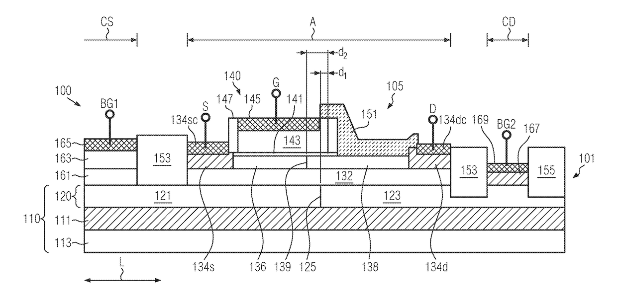
[0014]In the following description, for the purposes of explanation, numerous specific details are set forth in order to provide a thorough understanding of exemplary embodiments. It should be apparent, however, that exemplary embodiments may be practiced without these specific details or with an equivalent arrangement. In other instances, well-known structures and devices are shown in block diagram form in order to avoid unnecessarily obscuring exemplary embodiments. In addition, unless otherwise indicated, all numbers expressing quantities, ratios and numerical properties of ingredients, reaction conditions and so forth used in the specification and claims are to be understood as being modified in all instances by the term “about.”

[0015]Various illustrative embodiments of the invention are described below. In the interest of clarity, not all features of an actual implementation are described in this specification. It will of course be appreciated that in the development of any suc...


PUM


Abstract

The present disclosure provides a semiconductor device structure including an active region having a semiconductor-on-insulator (SOI) configuration, a semiconductor device of lateral double-diffused MOS (LDMOS) type, a dual ground plane region formed by two well regions which are counter-doped to each other, the dual ground plane region extending below the semiconductor device, and a deep well region extending below the dual ground plane region. Herein, the semiconductor device of LDMOS type comprises a gate structure formed on the active region, a source region and a drain region formed in the active region at opposing sides of the gate structure, and a channel region and a drift region, both of which being formed in the active region and defining a channel drift junction, wherein the channel drift junction is overlain by the gate structure.

Description

BACKGROUND1. Field of the Disclosure[0001]The present disclosure relates to semiconductor device structures at advanced technology nodes, such as 28 nm and beyond.2. Description of the Related Art[0002]As the world becomes more and more integrated through billions of connected devices, many emerging applications demand a new approach to semiconductor innovation. The chips that make these applications possible are evolving into mini-systems, with increased integration of intelligent components including wireless connectivity, non-volatile memory and power management, all while driving ultra-low power consumption. Current efforts aim at developing new standards for system integration, providing an optimized platform for combining various different applications, such as radio frequency (RF), analog, embedded memory and advanced logic onto a single chip, requiring a wide range of dynamic voltage scaling and unmatched design flexibility via software-controlled transistors capable of deli...

Claims


Application Information

Patent Timeline
IPC IPC(8): H01L29/78H01L29/10H01L29/06H01L29/40
CPCH01L29/7824H01L29/1095H01L29/408H01L29/0649H01L29/1083H01L21/28052H01L29/4933H01L29/4983H01L29/665H01L29/66689H01L29/78648H01L29/0653H01L21/84H01L29/78624H01L29/402
Inventor SCHIPPEL, CHRISTIANSIDELNICOV, ANDREIZSCHAETZSCH, GERD
Owner GLOBALFOUNDRIES US INC
Learn More