Unlock instant, AI-driven research and patent intelligence for your innovation.

OLED display and manufacturing method thereof

Active Publication Date: 2018-07-26
WUHAN CHINA STAR OPTOELECTRONICS TECH CO LTD
View PDF0 Cites 12 Cited by
  • Summary
  • Abstract
  • Description
  • Claims
  • Application Information

AI Technical Summary

Benefits of technology

The present invention provides an OLED display and a manufacturing method using a thin film encapsulation layer with a diamond-like carbon (DLC) layer for effective protection against moisture and oxygen from the lateral sides and for improving the light transmission of top emission devices. The DLC layer covers the steps formed between the organic buffer layer and the inorganic passivation layer, which prevents external moisture and oxygen from attacking the OLED device from the lateral side and ensures the light emitted by the device is not lost. The invention provides an OLED display with a longer service life and not affecting the brightness of the OLED device.

Problems solved by technology

However, the organic material is susceptible to reaction with moisture and oxygen and thus, a display based that is based on the organic material is subject to extremely severe requirement for packaging of an OLED display panel.
Such processes are not fit for flexible devices.
Although such a package structure effectively blocks corrosion caused by external moisture and oxygen, similar to the previously mentioned patent document, this package means lacks clear explanation of the relationship between moisture / oxygen resistance capability and transmission rate of DLC.
However, no detailed description is given in this patent document regarding techniques for manufacturing DLC and other inorganic layers.
This increases optical loss and lowers down the performance of a device.
However, such package arrangements all result in contradiction between moisture / oxygen blocking capability and transmission rate of DLC.

Method used


Image

  • OLED display and manufacturing method thereof
  • OLED display and manufacturing method thereof
  • OLED display and manufacturing method thereof

Examples


Embodiment Construction

[0066]To further expound the technical solution adopted in the present invention and the advantages thereof, a detailed description will be given with reference to the preferred embodiments of the present invention and the drawings thereof.

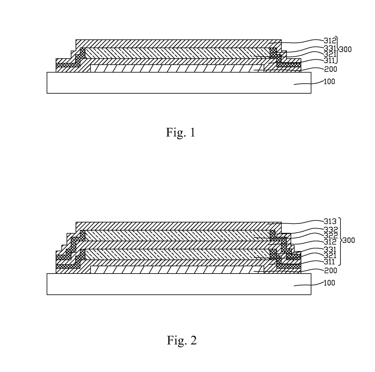
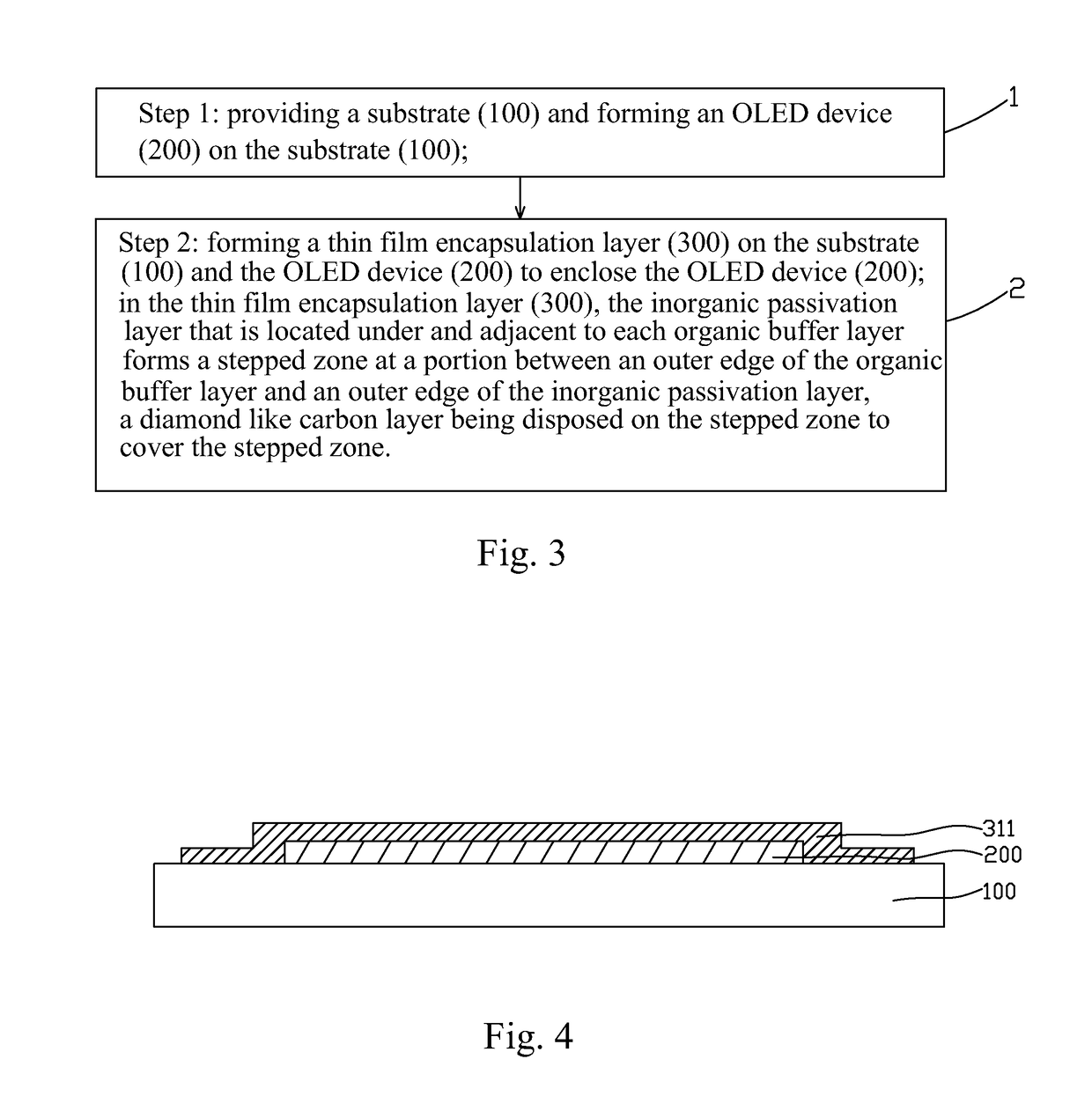
[0067]Referring to FIG. 1, which is a schematic view showing the structure of a first embodiment of an organic light-emitting diode (OLED) display according to the present invention, in the instant embodiment, the OLED display comprises a substrate 100, an OLED device 200 arranged on the substrate 100, and a thin film encapsulation layer 300 arranged on the substrate 100 and the OLED device 200 and enclosing the OLED device 200.

[0068]The thin film encapsulation layer 300 comprises at least two inorganic passivation layers, at least one organic buffer layer, and at least one diamond like carbon (DLC) layer. In the thin film encapsulation layer 300, each DLC layer corresponds to and belongs to the same layer as one organic buffer layer, while the in...


PUM


Abstract

The present invention provides an OLED display and a manufacturing method thereof. The OLED display of the present invention is such that in a thin film encapsulation layer, an inorganic passivation that is located under and adjacent to each organic buffer layer forms a stepped zone at a portion between an outer edge of the organic buffer layer and an outer edge of the inorganic passivation layer and each stepped zone is provided with a DLC layer that covers the stepped zone. In other words, the present invention uses DLC for later side encapsulation and in the thin film encapsulation layer, each organic buffer layer is provided, on an outer side thereof, with a DLC layer to thereby effectively block external moisture and oxygen from attacking the OLED device from a lateral side and also to eliminate an issue of loss for light of a top emission device to travel through DLC.

Description

BACKGROUND OF THE INVENTION1. Field of the Invention[0001]The present invention relates to the field of flat panel display technology and more particular to an organic light-emitting diode (OLED) display and a manufacturing method thereof.2. The Related Arts[0002]OLED displays possess advantages, such as being self-luminous, high brightness, wide view angle, high contrast, being flexible, and low power consumption, and thus attract much attention as a new generation of displaying solution that gradually takes the place of traditional liquid crystal displays. It is now a symbol of being high tech by adopting an OLED display panel from small size ones used in mobile phone display screens to large size ones used in high definition flat panel televisions.[0003]The OLED based display technology is different from the traditional liquid crystal display technology in that no backlighting is necessary and an extremely thin organic material coating layer and a glass substrate are involved so ...

Claims


Application Information

Patent Timeline
IPC IPC(8): H01L51/52H01L51/56
CPCH01L51/5246H01L51/56H01L51/5256H05B33/04H01L51/5237H01L51/524H01L51/5253H10K50/8445H10K50/844H10K71/00H10K50/8426H10K50/84H10K50/841
Inventor JIN, JIANGJIANGHSU, HSIANGLUN
Owner WUHAN CHINA STAR OPTOELECTRONICS TECH CO LTD