Semiconductor device and method of manufacturing the same

a technology of semiconductor devices and semiconductor films, applied in semiconductor devices, semiconductor/solid-state device details, electrical equipment, etc., can solve problems such as difficulty in forming copper films, difficulty close to being solved, and apparatus problems such as shallow penetration

Inactive Publication Date: 2005-05-10
SEMICON ENERGY LAB CO LTD
View PDF8 Cites 29 Cited by
  • Summary
  • Abstract
  • Description
  • Claims
  • Application Information

AI Technical Summary

Benefits of technology

[0018]The present invention has been made to solve the above-described problems of prior art, and an object of the present invention is therefore to provide a simple technique of forming a low-resistant wire in place of a Damascene method. In other words, an object of the present invention is to provide a semiconductor device obtained by using a simple technique of forming a low-resistant wire in place of a Damascene method as well as a method of manufacturing the semiconductor device.
[0044]In the invention having the above structure, the gate insulating film is a nitrogen-containing insulating film, specifically, a silicon oxynitride film, obtained by forming a silicon oxide film by deposition and then heating the film in an atmosphere that contains a nitrogen component (nitrogen as a molecule or as an element) to introduce nitrogen as an element into the gate insulating film. By introducing nitrogen as an element into the silicon oxide film, the gate insulating film gains a function of effectively preventing diffusion of copper or other low-resistant metal elements from the low-resistant metal portion (or the low-resistant metal film) provided in the gate electrode (or the laminate gate electrode). The insulating film on the second layer metal film may be a silicon nitride film, or a silicon oxynitride film, or a silicon oxide film.
[0047]According to the invention structured as above, the gate electrode (or the laminate gate electrode) is composed of a first layer metal film electrode (or a first layer metal film), a second layer metal film electrode (or a second layer metal film), and a low-resistant metal portion (or a low-resistant metal film). The first layer metal film electrode has a given measure in the channel length direction and is formed of one material selected from the group consisting of Ta, TaN, TaSiN, TiN, TiSiN, W, WN, WSiN, WBN, TiW, and IrTa. The second layer metal film electrode is formed of aluminum or an alloy mainly containing aluminum, and is laid on upper layer of the first layer metal film electrode. The ends of the second layer metal film electrode are positioned a certain distance in from the ends of the electrode. The low-resistant metal portion is formed of copper or silver that is a metal element smaller in specific resistance than aluminum, and is attached to each of left and right side wall portions of the second layer metal film electrode. Owing to the resistance lowering effect of copper or silver in the low-resistant metal portion (or the low-resistant metal film), the gate electrode (or the laminate gate electrode) as a whole has an electric resistance lower than that of aluminum. With nitrogen as an element introduced, the gate insulating film can effectively prevent diffusion of copper or silver as an element from the low-resistant metal portion and also is effective in stabilizing electric characteristics of the semiconductor device. The electric field relieving region is placed in the semiconductor layer so as to overlap an end of the gate electrode (or the laminate gate electrode) to give the TFT the GOLD structure. This improves the reliability against hot carriers.

Problems solved by technology

On the other hand, the dual Damascene method has difficulty in forming a copper film by embedding in a connection portion of high aspect ratio (aspect ratio: 3 to 5).
However, this difficulty is close to being solved because lately a technique of forming a copper film by embedding using electroplating has been established for a connection hole of high aspect ratio.
While the ArF excimer laser reduced projection exposure apparatus is capable of resolving an ultramicro pattern of 0.2 μm or less, the apparatus has a problem of shallow penetration.
However, despite their high electric field effect mobility, polycrystalline silicon TFTs sometimes suffer lowering of electric field effect mobility when continuously driven, as well as reduction in ON current (current flowing when a TFT is ON), an increase in OFF current (current flowing when a TFT is OFF), and other degradation symptoms, resulting in reliability problems.
On the other hand, the LDD structure is large in resistance of low-concentration impurity region (n− region or p− region) and therefore has a drawback of reduced drain current.
Accordingly, the low-concentration impurity region (n− region or p− region) is depleted and the resistance is increased, indicating a degradation mode unique to LDD, which has become a problem.
The above problems become noticeable as the channel length is shortened.
While the LDD structure has an advantage of small OFF current, it has a drawback of being less effective in repressing hot carriers by relieving an electric field near a drain.
However, the GOLD structure has a drawback of large OFF current.
However, the Damascene method has a problem of unusual scratch defects such as erosion and dishing generated on a surface polished in a CMP process for polishing a thick copper film that has been formed by electroplating.
This leads to problems in yield and reliability.
Although the scratch defects such as erosion and dishing described above are reduced by improvement of the CMP process, it is far from solving the problem completely.

Method used


Image

  • Semiconductor device and method of manufacturing the same
  • Semiconductor device and method of manufacturing the same
  • Semiconductor device and method of manufacturing the same

Examples


embodiment mode 1

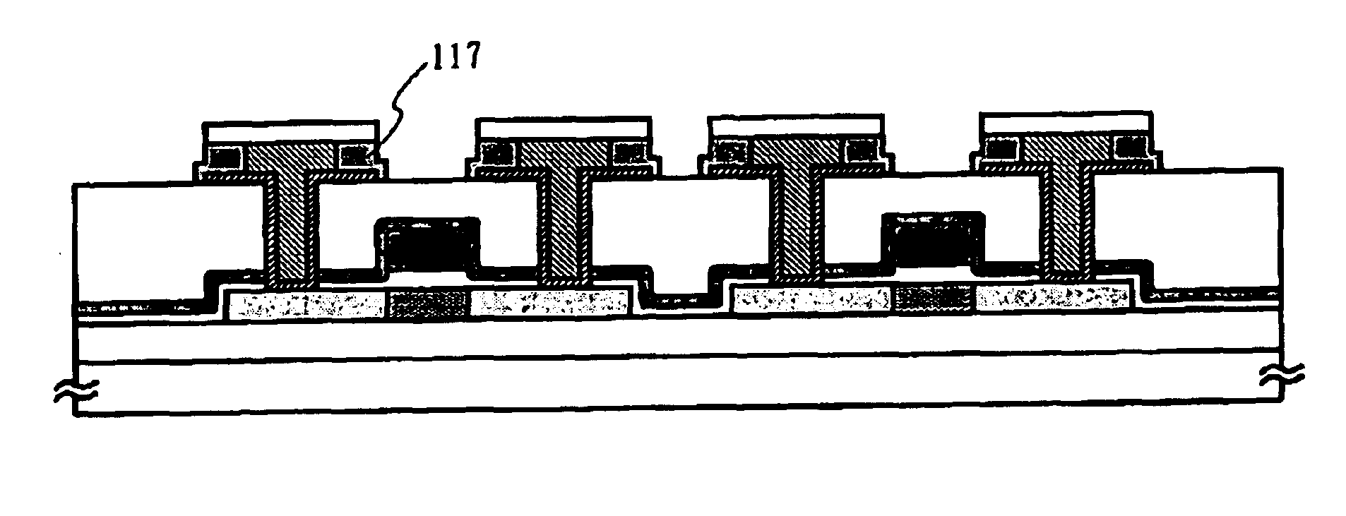
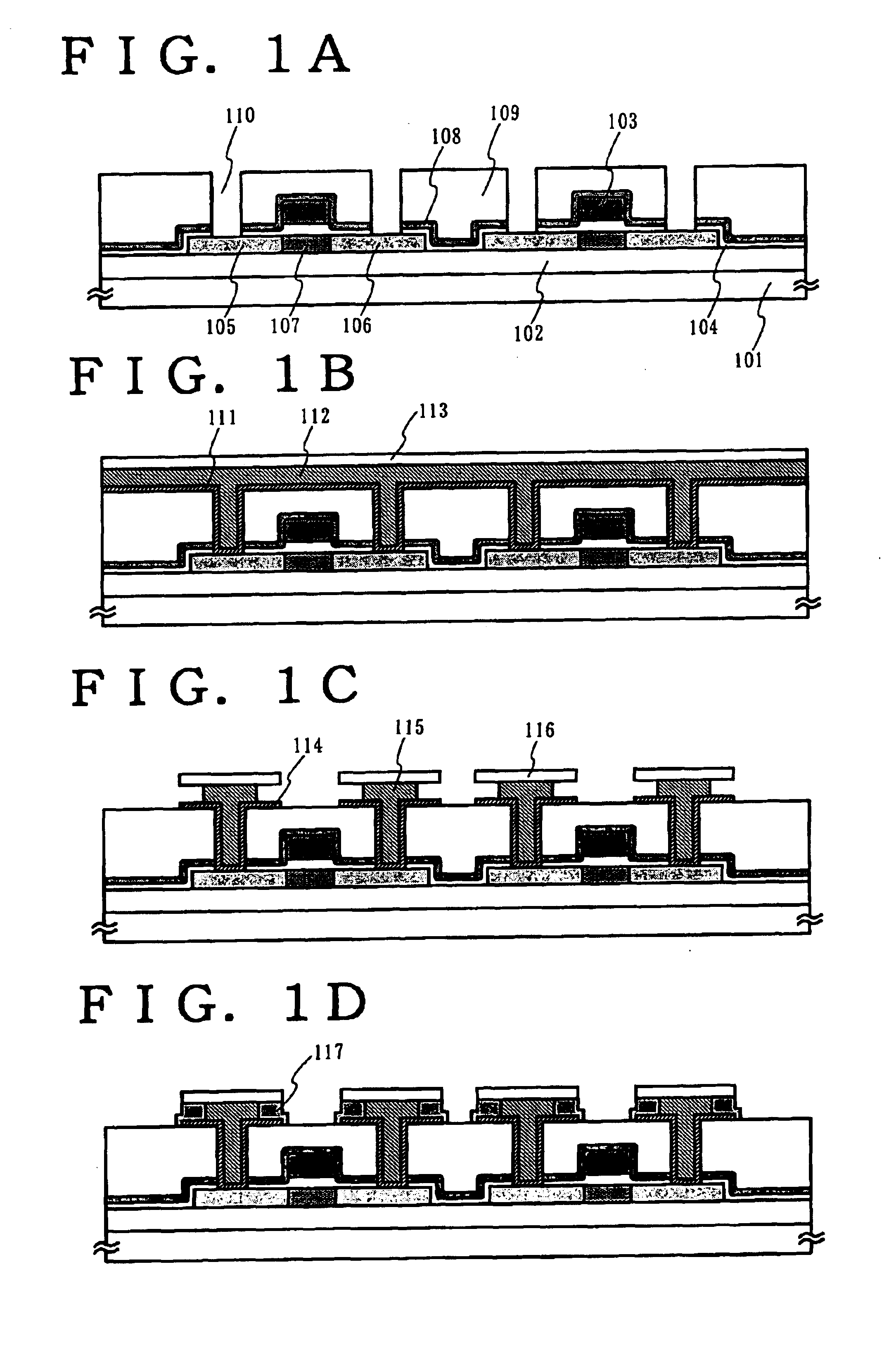
[0064]This embodiment mode describes, as a specific example of a semiconductor device and its manufacture method, a case of applying the present invention to wires that are connected to a source electrode and drain electrode of a TFT on a transparent insulating substrate. The description will be given with reference to FIGS. 1A to 1D.

[0065]The structural aspect of the semiconductor device is described first.

[0066]According to the basic structure used in this embodiment mode, a base film 102 is formed by deposition on a glass substrate 101 that is a transparent insulating substrate. The base film 102 is a silicon oxynitride film with a given thickness for preventing diffusion of impurity elements from the glass substrate 101. On the base film 102, a TFT is formed as a semiconductor element. The TFT is composed of a gate electrode 103, a gate insulating film 104, and a semiconductor layer. The gate electrode 103 is formed of an aluminum-based alloy or an alloy of a high-melting point ...

embodiment mode 2

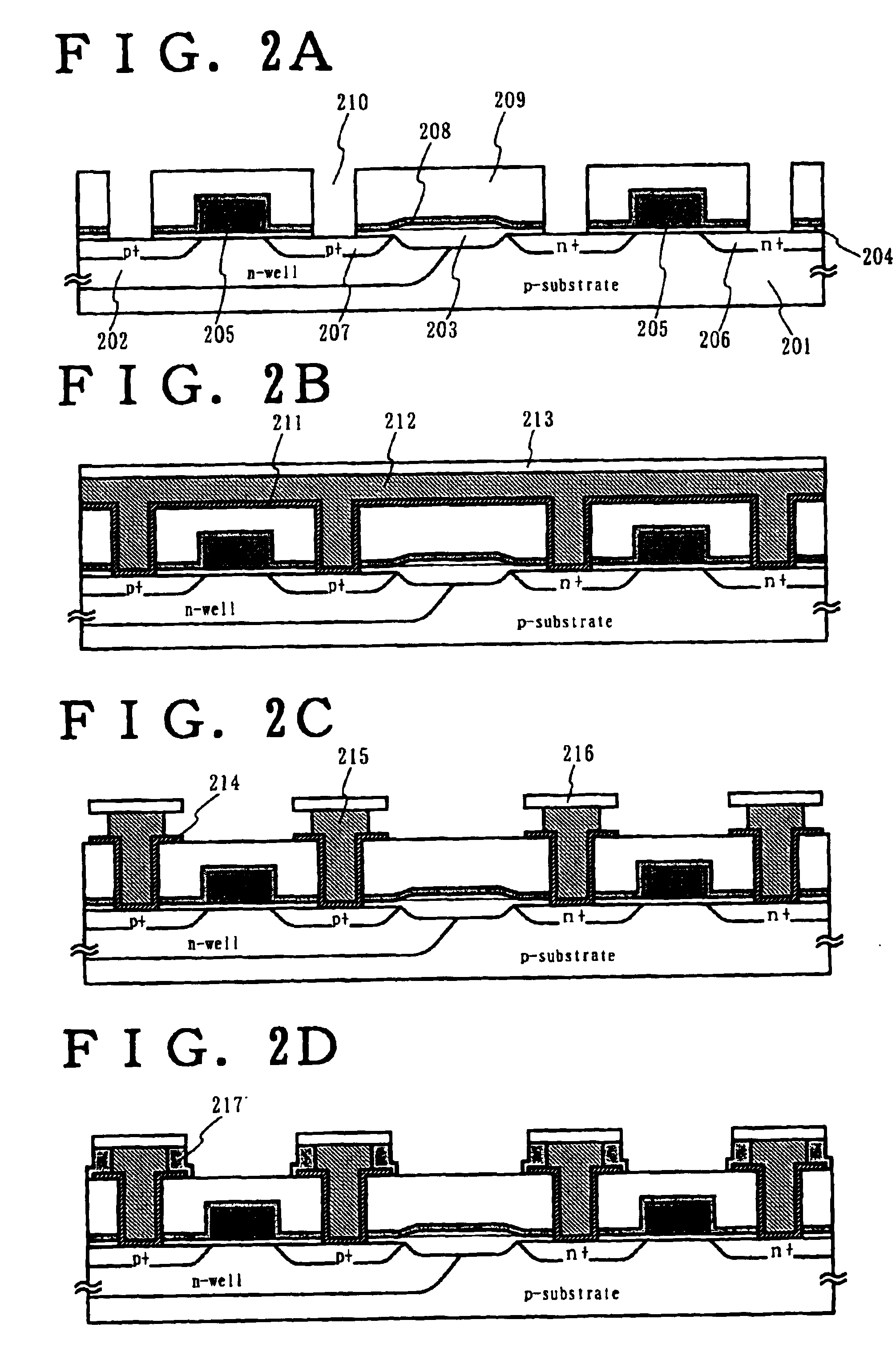
[0079]This embodiment mode describes an example of applying the present invention to wires connected to a source electrode and drain electrode of a CMOS transistor on a semiconductor substrate. The description will be given with reference to FIGS. 2A to 2D. The description in this embodiment mode focuses on the structure of the CMOS transistor, and explanations on the structure and manufacture method of the wires are omitted or simplified to avoid repetition of Embodiment Mode 1.

[0080]A semiconductor element is formed on a p type silicon substrate 201 that is a semiconductor substrate. The semiconductor element is a CMOS structure transistor having an NMOS transistor and a PMOS transistor. The NMOS transistor is formed on a p type region and therefore it is not necessary to form a well structure in the p type silicon substrate 201. On the other hand, the PMOS transistor is formed on an n type region. Therefore the PMOS transistor is formed in an n well region 202 where a low concent...

embodiment mode 3

[0089]This embodiment mode is about an example of applying a wire with a low-resistant metal portion attached thereto to a gate electrode of an n-channel TFT. A specific description will be given below with reference to FIGS. 3A to 3E.

[0090]The structural aspect of a semiconductor device is described first.

[0091]In a semiconductor device of the present invention, a base film 302 is formed by deposition on a glass substrate 301 that is a transparent insulating substrate. The base film 302 is a film with a given thickness for preventing diffusion of impurity elements from the glass substrate 301, specifically a silicon oxynitride film with a thickness of 100 to 200 nm. Formed on the base film 302 is an n-channel TFT with a gate electrode having a low-resistant metal portion 315. The TFT is composed of the gate electrode, a gate insulating film 304b, and a semiconductor layer 303. The gate electrode has an electric resistance smaller than that of aluminum. The gate insulating film 304b...


PUM

PropertyMeasurementUnit
wavelengthaaaaaaaaaa
temperatureaaaaaaaaaa

Abstract

A simple technique of forming a low-resistant wire is provided in place of a Damascene method. In a three-layer wire composed of a first layer metal film wire, a second layer metal film wire that has fixed side etching portions, and an insulating film pattern, a low-resistant metal such as copper or silver is deposited in concave regions corresponding to the side etching portions of the second layer metal film wire through electrodeposition by electroplating. The above process is applied to a gate electrode and wire of a semiconductor device to obtain a semiconductor device that has high operation speed.

Description

BACKGROUND OF THE INVENTION[0001]1. Field of the Invention[0002]The present invention relates to a semiconductor device and a method of manufacturing the same, specifically to a semiconductor device having a low-resistant metal wire that is formed by using an electroplating technique and a method of manufacturing the semiconductor device. The term semiconductor device refers to devices in general that utilize semiconductor characteristics to function, and it includes a large-scale integrated circuit fabricated on a semiconductor substrate, a semiconductor display device in which circuits are built from thin film transistors formed on a transparent insulating substrate, and the like.[0003]2. Description of the Related Art[0004]Related art of the present invention are a technique of forming a copper (Cu) wire by a Damascene method in a large-scale integrated circuit (hereinafter abbreviated as LSI) and a technique of forming a thin film transistor (hereinafter abbreviated as TFT) that...

Claims


Application Information

Patent Timeline
Patent Type & Authority Patents(United States)
IPC IPC(8): H01L21/02H01L21/288H01L21/70H01L29/45H01L29/66H01L29/786H01L21/84H01L21/768H01L27/12H01L29/40H01L21/28H01L21/3205H01L21/77H01L21/8238H01L23/52H01L27/092H01L29/423H01L29/43H01L29/49H01L29/78
CPCH01L21/2885H01L21/76838H01L21/76843H01L21/76852H01L27/12H01L29/458H01L29/78621H01L27/124H01L27/1292H01L2924/0002H01L2924/00
Inventor SUGAWARA, AKIRATANAKA, NOBUHIROUEHARA, ICHIRO
Owner SEMICON ENERGY LAB CO LTD
Why Eureka
Try Eureka