Class d amplifier

a class d amplifier and amplifier technology, applied in amplifiers, amplifiers with semiconductor devices/discharge tubes, amplifier modifications to reduce non-linear distortion, etc., can solve the problems of not providing a technology for attaining advantages, not disclosing at all a standard according, and occurrence of beats, so as to reduce switching losses, improve efficiency, and reduce oscillation frequency

Active Publication Date: 2018-08-09
YAMAHA CORP
View PDF0 Cites 4 Cited by
  • Summary
  • Abstract
  • Description
  • Claims
  • Application Information

AI Technical Summary

Benefits of technology

[0010]With this disclosure, in the case that the level of the reference signal indicating the driving amount for the load at the output stage is smaller than the threshold value, the carrier signal is supplied to the comparator as the standard signal, whereby the class D amplifier operates as a separately-excited class D amplifier. On the other hand, in the case that the level of the reference signal is the threshold value or more, a predetermined standard potential is supplied to the comparator as a standard signal, whereby the class D amplifier operates as a self-excited class D amplifier. Hence, with this disclosure, the class D amplifier operates as a separately-excited class D amplifier at the time of no signal or small output, thereby being capable of preventing the occurrence of a beat, and operates as a self-excited class D amplifier at the time of large output, thereby being capable of reducing switching loss and improving efficiency by lowering the oscillation frequency and being capable of enhancing audio performance by reducing the distortion rate.

Problems solved by technology

JP-UM-B-3129456, however, does not disclose at all a standard according to which the switching between the operation as a self-excited class D amplifier and the operation as a separately-excited class D amplifier is performed.
In JP-A-2005-269580, however, switching operation at a fixed frequency similar to that of a separately-excited class D amplifier is performed by the self-excited class D amplifier, whereby JP-A-2005-269580 does not provide a technology for attaining the advantages of both the self-excited class D amplifier and the separately-excited class D amplifier.
However, when the self-excited class D amplifiers for a plurality of channels are operated simultaneously, the difference components due to the individual differences in the oscillation frequencies of the respective amplifiers cause the occurrence of a beat.
At the time of no signal or small output, since the oscillation frequency of the self-excited oscillation of the self-excited class D amplifier does not change, this beat is easily audible and is liable to become a problem.
On the other hand, although the separately-excited class D amplifier generates no beat, since the amplifier performs, at the time of large output, switching operation at a fixed frequency similar to that at the time of no signal or small output, the amplifier is large in switching loss and low in efficiency in comparison with the self-excited class D amplifier.
Hence, the separately-excited class D amplifier is not suitable as a large output amplifier.
Still further, since the separately-excited class D amplifier has a small feedback amount, enhancing audio performance by lowering the distortion rate is difficult.

Method used


Image

  • Class d amplifier
  • Class d amplifier
  • Class d amplifier

Examples


first embodiment

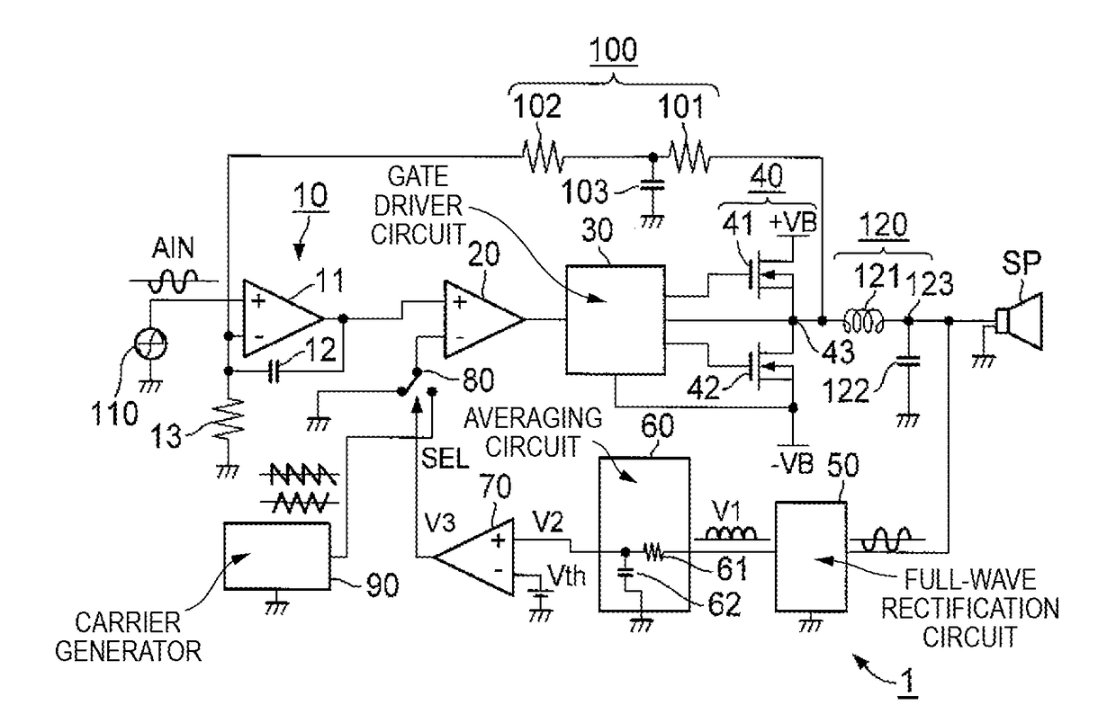
[0024]FIG. 1 is a circuit diagram showing a configuration of a class D amplifier 1 according to a first embodiment of this disclosure. In FIG. 1, a speaker SP serving as the load of the class D amplifier 1 and a filter 120 interposed between the class D amplifier 1 and the speaker SP are also shown to facilitate the understanding of the configuration of the class D amplifier 1.

[0025]As shown in FIG. 1, the class D amplifier 1 has an integration amplifier 10, a comparator 20, a gate driver circuit 30, an output stage 40, a full-wave rectification circuit 50, an averaging circuit 60, a comparator 70, a switch 80, a carrier generator 90, and a feedback circuit 100.

[0026]The integration amplifier 10 has an operational amplifier 11, a capacitor 12, and a resistor 13. The input audio signal AIN from an audio signal source 110 is given to the non-inverting input terminal (plus input terminal) of the operational amplifier 11. An integrating capacitor 12 is interposed between the output term...

second embodiment

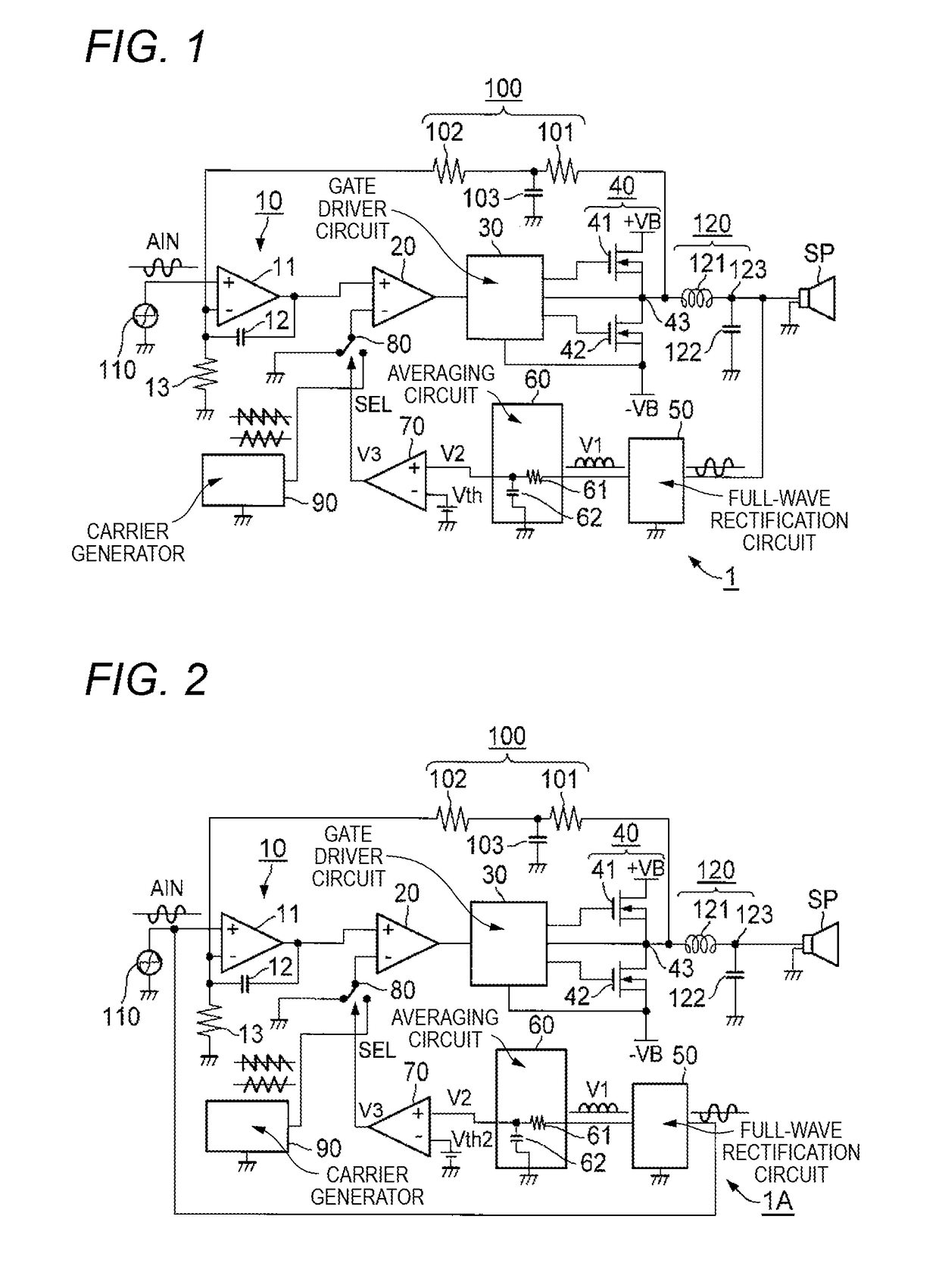
[0055]FIG. 2 is a circuit diagram showing a configuration of a class D amplifier 1A according to a second embodiment of this disclosure. In the above-mentioned first embodiment, the reference signal generator having the full-wave rectification circuit 50 and the averaging circuit 60 generates the reference signal V2 on the basis of the drive signal for the speaker SP. On the other hand, in the class D amplifier 1A according to this embodiment, the reference signal generator having the full-wave rectification circuit 50 and the averaging circuit 60 generates the reference signal V2 on the basis of the input audio signal AIN. This is because the level of the drive signal for the speaker SP depends on the level of the input audio signal AIN. This embodiment is different from the above-mentioned first embodiment in this respect.

[0056]In this embodiment, the averaging circuit 60 outputs a DC voltage corresponding to the average value of the full-wave rectified voltage V1 of the input aud...

third embodiment

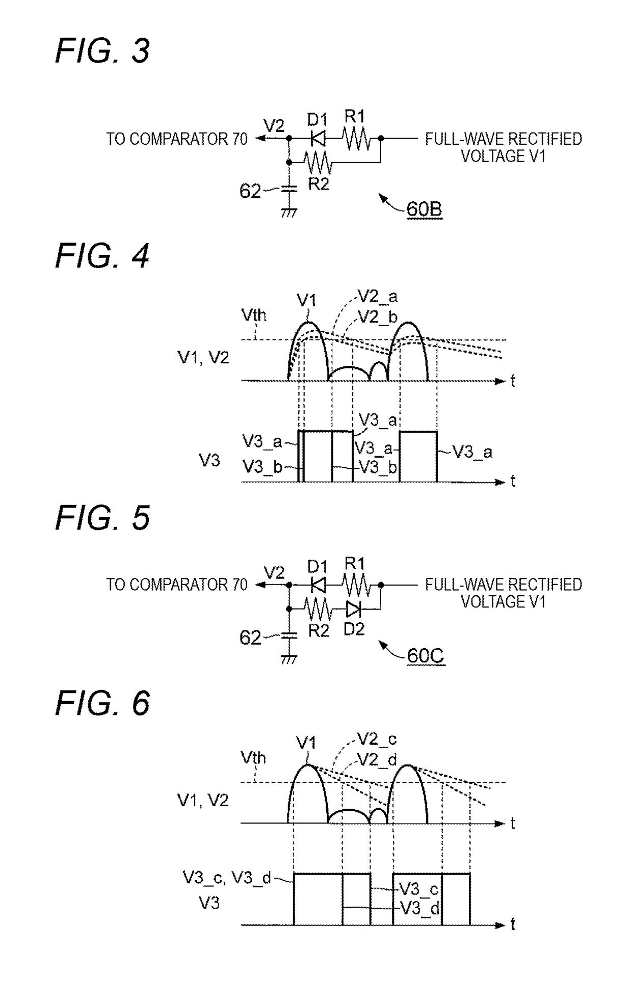
[0058]Next, a third embodiment of this disclosure will be described. In this embodiment, the averaging circuit 60 in the above-mentioned first or second embodiment is replaced with an averaging circuit 60B shown in FIG. 3. This averaging circuit 60B is configured such that the resistor 61 of the averaging circuit 60 (see FIGS. 1 and 2) is replaced with a circuit having a diode D1, a resistor R1 and a resistor R2. As shown in FIG. 3, one terminal of the resistor R1 and one terminal of the resistor R2 are commonly connected, and the full-wave rectified voltage V1 from the full-wave rectification circuit 50 (see FIGS. 1 and 2) is given to this common connection point. The other terminal of the resistor R1 is connected to the anode of the diode D1, and the cathode of the diode D1 and the other terminal of the resistor R2 are commonly connected to an electrode of the capacitor 62 connected to the comparator 70.

[0059]In FIG. 3, in the case that the full-wave rectified voltage V1 is higher...


PUM


Abstract

A class D amplifier includes an output stage that performs a switching operation, a feedback circuit that generates a feedback signal based on the output signal output from the output stage, an integration amplifier that outputs an integrated value signal in response to an input signal and the feedback signal, a comparator that compares the integrated value signal with a standard signal, a driver that controls the output stage based on a signal output from the comparator, a carrier signal generator that generates a carrier signal, a reference signal generator that outputs a reference signal indicating a driving amount for a load at the output stage, and a standard signal switch that switches the standard signal to the carrier signal or a standard potential based on whether a level of the reference signal is smaller than a threshold value.

Description

CROSS REFERENCE TO RELATED APPLICATIONS[0001]This application is a continuation of PCT application No. PCT / JP2016 / 079645, which was filed on Oct. 5, 2016 based on Japanese Patent Application (No. 2015-197330) filed on Oct. 5, 2015, the contents of which are incorporated herein by reference.BACKGROUND OF THE INVENTION1. Field of the Invention[0002]This disclosure relates to a class D amplifier suitable as a power amplifier for driving a speaker.2. Description of the Related Art[0003]In recent years, class D amplifiers have come into wide use as power amplifiers for audio use. These class D amplifiers are amplifiers in which output stage transistors are ON / OFF switched by a PWM pulse train that is pulse-width modulated depending on an input audio signal and the current from a power source is supplied to a speaker via these output stage transistors.[0004]These class D amplifiers are available as an amplifier being configured so as to generate the above-mentioned PWM pulse train by usin...

Claims


Application Information

Patent Timeline
Patent Type & Authority Applications(United States)
IPC IPC(8): H03F3/217
CPCH03F3/2173H03F3/185H03F2200/03H03F2200/351H03F1/0205H03F1/32H03F3/2171
Inventor MIYAKE, YOSHIRO
Owner YAMAHA CORP
Why Eureka
Try Eureka