
In-cell touch display panel and electronic device

Active Publication Date: 2018-08-16
WUHAN CHINA STAR OPTOELECTRONICS TECH CO LTD
View PDF0 Cites 1 Cited by
  • Summary
  • Abstract
  • Description
  • Claims
  • Application Information

AI Technical Summary

Benefits of technology

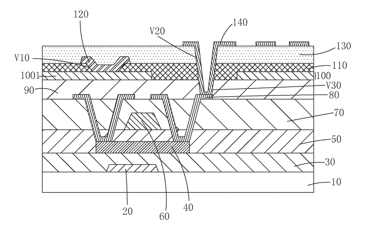
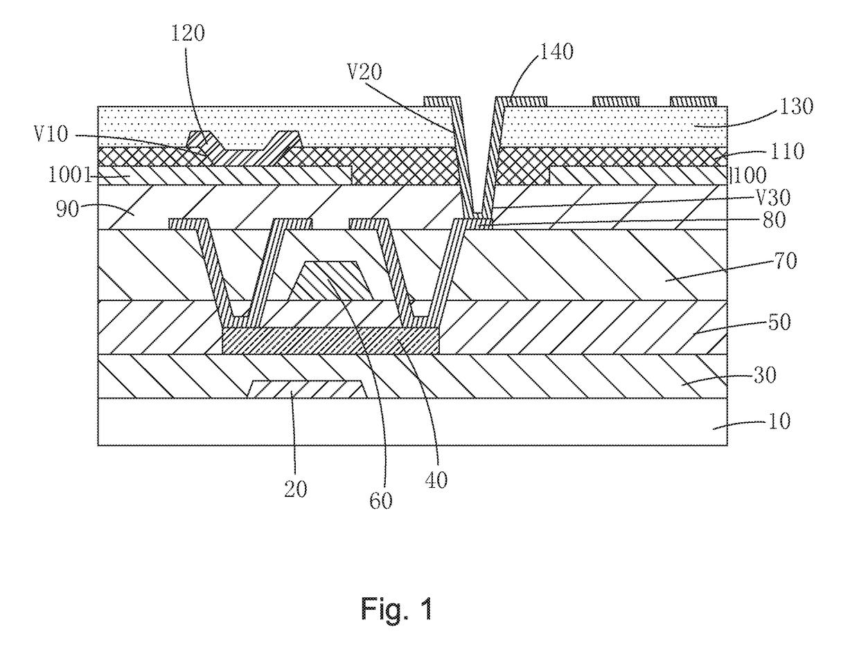
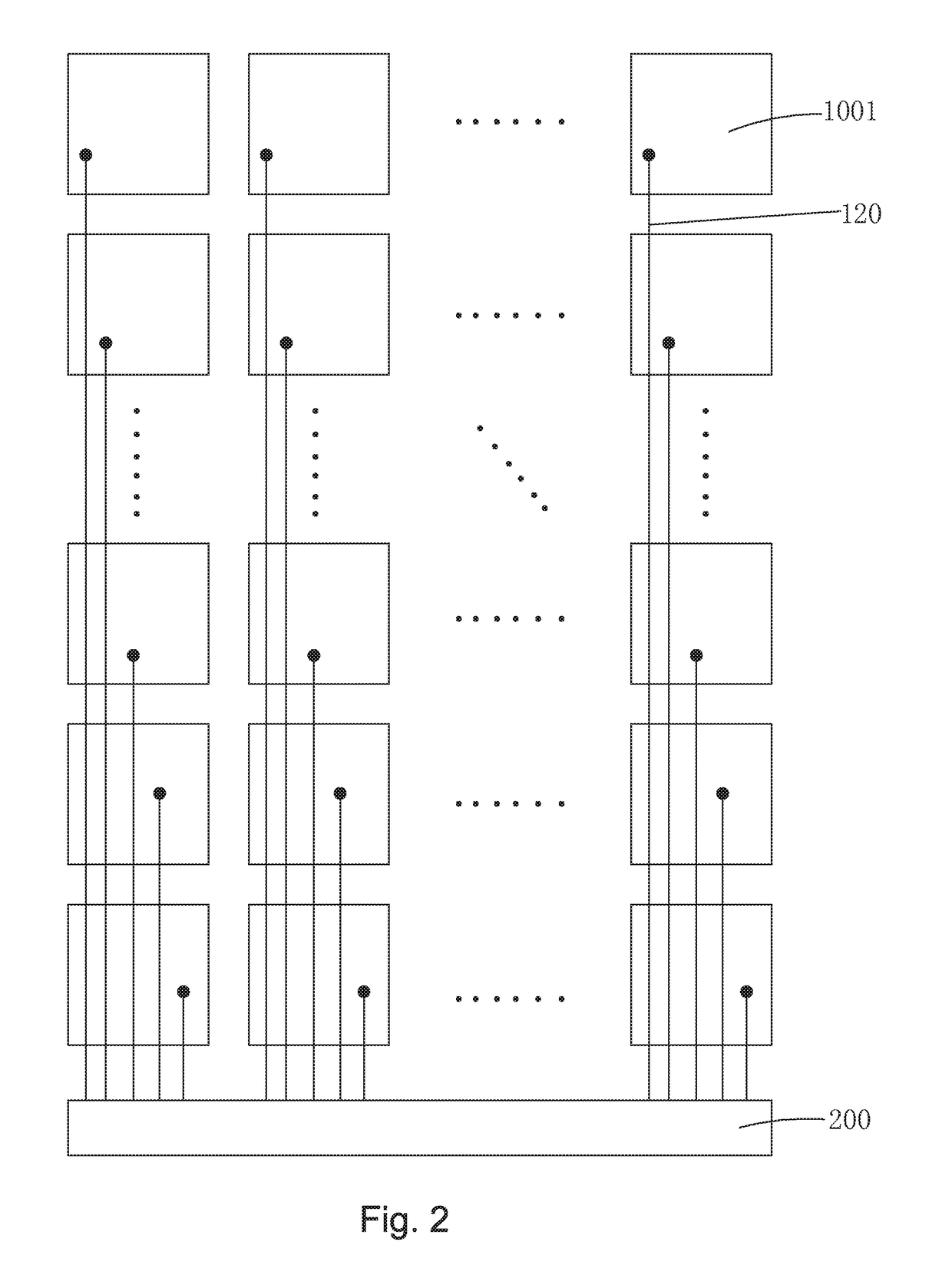
This patent is about a new way to create touch display panels for electronic devices. The new method uses fewer masks and processes, reducing production costs and improving efficiency and touch performance. The positions of the electrodes are switched, with the common electrode layer becoming the top layer and the pixel electrode layer becoming the layer below it. This change in position means that the pixel electrode can connect to the TFT (the part that creates the image) without needing to drill through multiple layers. This saves money and improves production efficiency. Additionally, placing the common electrode as the touch sensor at the top layer allows for better sensitivity and signal-to-noise ratio, resulting in better touch performance and product quality.

Problems solved by technology

Although the touch display panel based on the conventional IMI architecture can realize the touch function, the manufacturing process requires more masks and more technical processes and results a higher production cost.

Method used


Image

  • In-cell touch display panel and electronic device
  • In-cell touch display panel and electronic device
  • In-cell touch display panel and electronic device

Examples


Embodiment Construction

[0031]To further explain the technique means and effect of the present invention, the following uses preferred embodiments and drawings for detailed description.

[0032]Referring to FIG. 3 and FIG. 4. The present invention provides an in-cell touch display panel, which comprises: a thin film transistor (TFT) array substrate 1, a color filter (CF) substrate 3 disposed opposite to the TFT array substrate 1, and a liquid crystal (LC) layer 5 sandwiched between the TFT array substrate 1 and the CF substrate 3.

[0033]The TFT array substrate 1 comprises: a glass base 11, a light-shielding layer 12 disposed on the glass base 11, a buffer layer 13 disposed on the glass base 11 and the light-shielding layer 12; a plurality of TFTs 14 arranged in an array and disposed on top of the buffer layer 13, a planarization layer 15 on top of the TFTs 14, a pixel electrode layer 16 disposed on top of the planarization layer 15, a protective layer 17 disposed on top of the pixel electrode layer 16, a metal...


PUM


Abstract

The invention provides a touch display panel and an electronic device, with the positions of pixel electrode layer and common electrode layer at the side of array substrate in conventional touch display panel changed; wherein common electrode layer (21) as touch sensor is changed to the top, and pixel electrode layer (16) is changed to below common electrode layer (21). Pixel electrode (16) is connected to source / drain (145) of TFT (14) via first through hole (V1) penetrating planarization layer (15), which requiring only to drill planarization layer without the need to drill both the protective layer and planarization layer as in prior art to achieve connecting pixel electrode to TFT. The invention saves a mask, a drilling process and production cost and improves production efficiency. Moreover, placing common electrode (21) as touch sensor at the top facilitates optimizing sensitivity and SNR, thereby improves touch performance and product quality.

Description

BACKGROUND OF THE INVENTION1. Field of the Invention[0001]The present invention relates to the field of touch display techniques, and in particular to an in-cell touch display panel and electronic device.2. The Related Arts[0002]The touch technology, as an important indicator of smart technology, is applied more and more widely. Through rapid development, the touch technology, in accordance with the principle of touch, can be divided into piezo-resistive, optical, capacitive, and so on, wherein the capacitive touch technology is the most widely used after gone through several generations of development. The capacitive touch technology can be divided into add-on type, on-cell type and in-cell type.[0003]At present, the in-cell touch display panels are increasingly used in mobile phones and other electronic display devices. The in-cell touch display panel integrates the touch function and the display function together by manufacturing the touch sensor between the thin film transistor ...

Claims


Application Information

Patent Timeline
IPC IPC(8): G06F3/041H01L27/12
CPCG06F3/0412H01L27/124G09G2310/0264G02F1/13338G02F1/134309G02F1/136227G06F3/044G06F2203/04103G02F1/133707G02F1/136209H01L29/78633G06F3/0443
Inventor ZHANG, HONGSENHUANG, YAOLI
Owner WUHAN CHINA STAR OPTOELECTRONICS TECH CO LTD
Learn More