Semiconductor devices and methods to enhance electrostatic discharge (ESD) robustness, latch-up, and hot carrier immunity

a technology of electrostatic discharge and shielding device, applied in the direction of shielding device, transistor, electrical apparatus, etc., can solve the problems of lowering the robustness of esd, device damage, and the price of lowering esd robustness in these advanced technology nodes, and achieve the highest latch-up immunity of parasitics, enhanced product reliability and life expectancy, selectively enhancing parasitic (scr/bipolar) action

Active Publication Date: 2018-08-30
INDIAN INSTITUTE OF SCIENCE
View PDF6 Cites 7 Cited by
  • Summary
  • Abstract
  • Description
  • Claims
  • Application Information

AI Technical Summary

Benefits of technology

[0018]It is an object of the present disclosure to provide a technological solution that achieves ESD efficient protection devices and ensures highest latch-up immunity of parasitic SCRs under the functional devices which can be across ESD protection devices in non-planar technologies.
[0019]It is an object of the present disclosure to provide enhanced product reliability and life expectancy.
[0020]It is an object of the present disclosure to provide a solution that can selectively enhance parasitic (SCR / Bipolar) action in intended parasitic / ESD devices, or can suppress the same in functional devices.
[0021]The present disclosure relates to the field of electrostatic discharge (ESD) protection devices. In particular, the present disclosure pertains to a mixed silicidation and selective epitaxy (EPI) fin field effect transistor (FinFET) processes that enables latch-up immunity together with ESD robustness. Also, the present disclosure pertains to a hybrid contact and junction profiles for FinFET technology that provides improved ESD robustness for ESD protection devices while achieving reliable I / O and core devices.

Problems solved by technology

US2015 / 0091090A1, and U.S. Pat. No. 7,888,775B2 provide prior art ways of implementing BJT and SCR-like devices in FinFET technologies provide various designs of diode FinFET (non-planar ESD diodes), however, due to inefficacy of heat dissipation mechanisms and much higher packing density of active area (Fins / Nanowires), these designs exhibit an increased self-heating over the device active area, which leads to an early failure, hence lowered ESD robustness.
Although, the advent of non-planar technologies has paved new and efficient ways to replace their planar counterparts by offering beneficial technological solutions to scale conventional transistors, this has come with a price of lowered ESD robustness in these advanced technology nodes.
Encountered during operation, latch-up is characterized as a high current condition where the device is irreversibly latched into a single electrical state typically preventing the entire circuit from functioning properly and resulting in device damage, if not complete destruction.
Thus, when random operational conditions such as electrical transients are encountered, regenerating feedback occurs with a resultant latch-up of the device's electrical state.
CMOS latch-up is a commonly recognized problem.
However, these methods are variously disadvantageous due to substantially increased device structure and fabrication process complexity, low degrees of reproducibility, excessive degradation of device's operating characteristics including substantially increased leakage currents, and, in particular, failure to reduce the parasitic feedback loop gain to less than one.
More specifically it is the inadvertent creation of a low-impedance path between power supply rails of a MOSFET circuit, triggering a parasitic structure that disrupts proper functioning of the part, possibly even leading to its destruction due to extremely high current.

Method used


Image

  • Semiconductor devices and methods to enhance electrostatic discharge (ESD) robustness, latch-up, and hot carrier immunity
  • Semiconductor devices and methods to enhance electrostatic discharge (ESD) robustness, latch-up, and hot carrier immunity
  • Semiconductor devices and methods to enhance electrostatic discharge (ESD) robustness, latch-up, and hot carrier immunity

Examples


Embodiment Construction

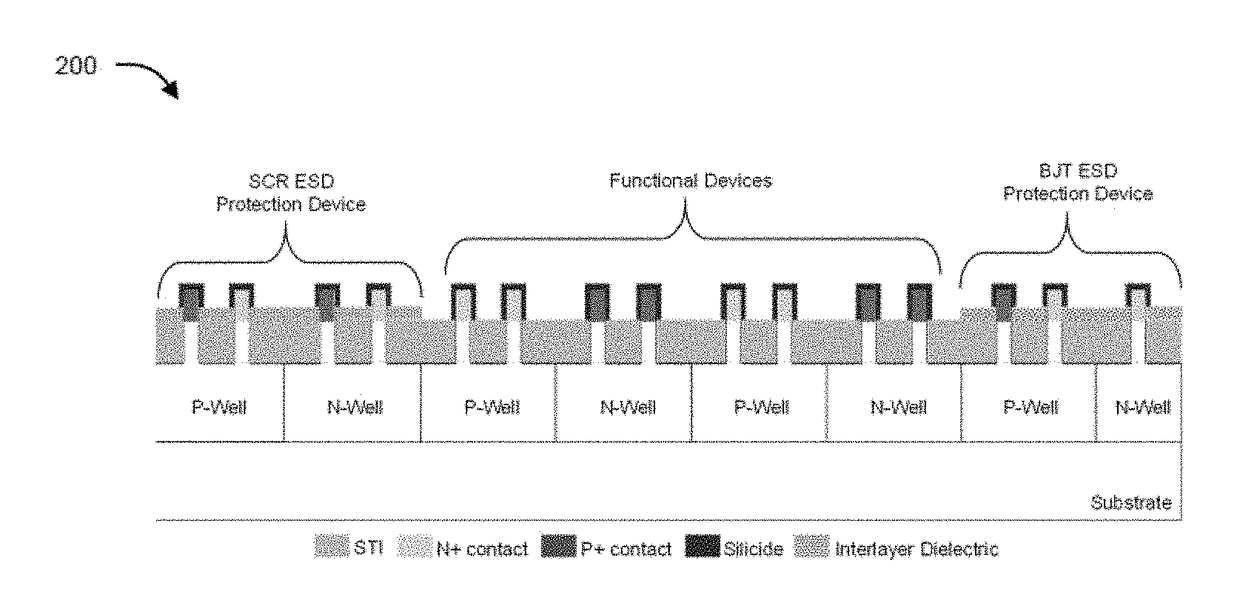
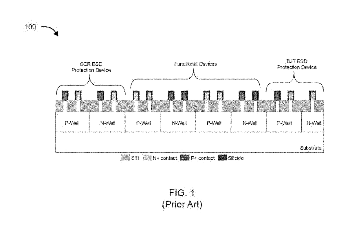
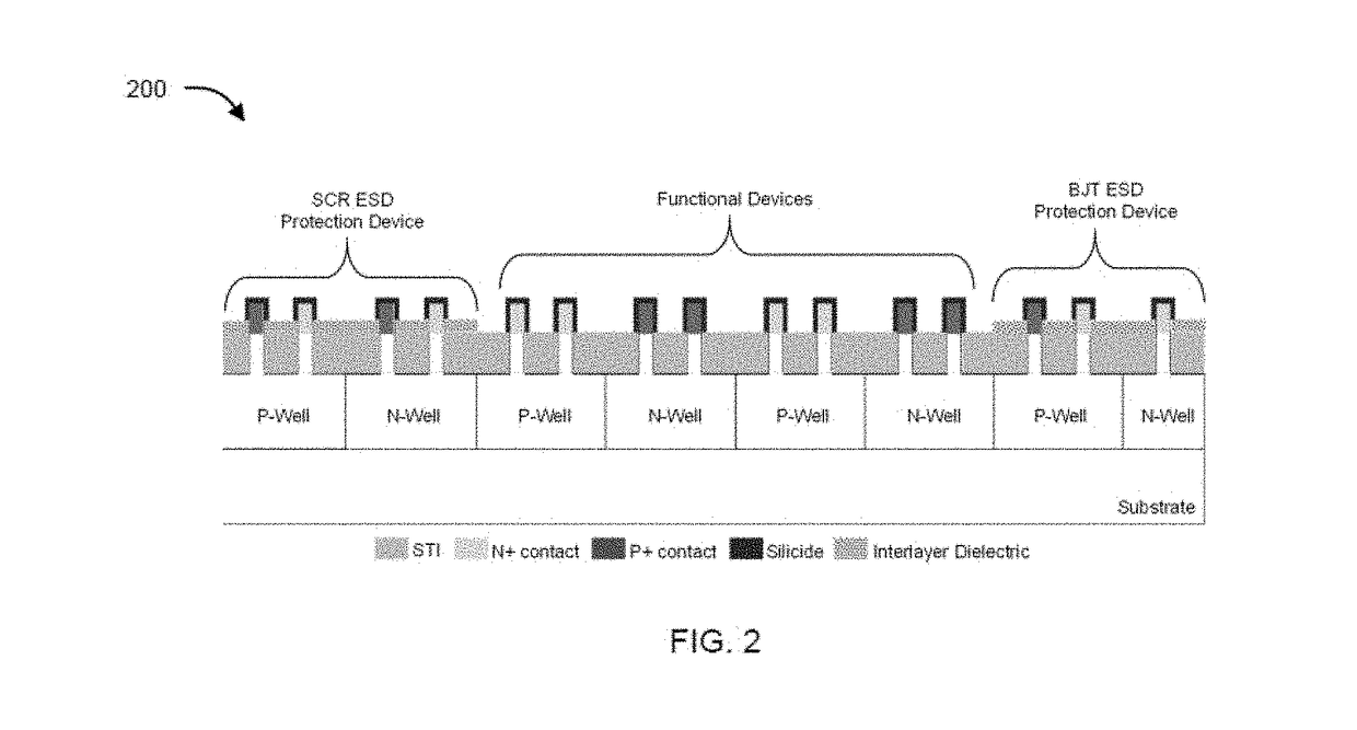
[0041]The following is a detailed description of embodiments of the disclosure depicted in the accompanying drawings. The embodiments are in such detail as to clearly communicate the disclosure. However, the amount of detail offered is not intended to limit the anticipated variations of embodiments, on the contrary, the intention is to cover all modifications, equivalents, and alternatives falling within the spirit and scope of the present disclosure as defined by the appended claims.

[0042]Each of the appended claims defines a separate invention, which for infringement purposes is recognized as including equivalents to the various elements or limitations specified in the claims. Depending on the context, all references below to the “invention” may in some cases refer to certain specific embodiments only. In other cases it will be recognized that references to the “invention” will refer to subject matter recited in one or more, but not necessarily all, of the claims.

[0043]Various ter...


PUM


Abstract

The present disclosure relates to non-planar ESD protection devices. The present disclosure provides a device structure and method of fabricating the structure that is essentially immune to latch-up and possess high ESD robustness and reliability. In an aspect, the present disclosure provides a mixed silicidation and selective epitaxy (epi) FinFET processes for latch-up immunity together with ESD robustness, thereby allowing achievement of ESD efficient parasitic structures together with latch-up immune and reliable functional devices. The present disclosure provides a dual silicidation scheme where ESD protection element(s) have fins that are partially silicided, and functional devices have fins that are fully silicided. The present disclosure also provides a hybrid contact and junction profile scheme where ESD protection element(s) have fins that are partially silicided with or without deep junctions depending on their application, and functional devices have fins that are fully silicided with the silicide edge crossing the junction. On the other hand, a dual Epi scheme is implemented such that ESD protection elements have fins with Epi contact, and functional devices have fins that are fully silicided without Epi (raised S/D) contact.

Description

TECHNICAL FIELD[0001]The present disclosure relates to the field of electrostatic discharge (ESD) protection devices. In particular, the present disclosure pertains to a mixed silicidation and selective epitaxy (EPI) fin field effect transistor (FinFET) processes that enables latch-up immunity together with ESD robustness.BACKGROUND[0002]Background description includes information that may be useful in understanding the present invention. It is not an admission that any of the information provided herein is prior art or relevant to the presently claimed invention, or that any publication specifically or implicitly referenced is prior art.[0003]There are many prior-art documents that provide different ways of designing non-planar ESD diodes. For example, US Patent documents U.S. Pat. No. 8,928,083B2. US2016 / 0020203A1. U.S. Pat. No. 7,560,784B2, US2014 / 0191319A1, US2006 / 0063334A 1, U.S. Pat. No. 7,964,893B2, US2014 / 0183641A1, U.S. Pat. No. 9,006,054B2, US2014 / 0252476A1, U.S. Pat. No. ...

Claims


Application Information

Patent Timeline
Patent Type & Authority Applications(United States)
IPC IPC(8): H01L27/02H01L27/088H01L27/12H01L29/78H01L29/74H01L21/8234
CPCH01L27/0266H01L27/088H01L27/1203H01L29/7843H01L29/7851H01L29/7436H01L21/823418H01L27/0262H01L21/823814H01L27/0623H01L27/0924H01L27/0921
Inventor SHRIVASTAVA, MAYANKPAUL, MILOVAGOSSNER, HARALD
Owner INDIAN INSTITUTE OF SCIENCE
Why Eureka
Try Eureka