Method of carrier profiling in semiconductors

a carrier profiling and semiconductor technology, applied in the field of semiconductor carrier profiling, to achieve the effect of reducing the types of lasers and reducing the effects of prior art limitations

Active Publication Date: 2018-09-27
HAGMANN MARK J
View PDF3 Cites 2 Cited by
  • Summary
  • Abstract
  • Description
  • Claims
  • Application Information

AI Technical Summary

Benefits of technology

[0008]In view of the foregoing disadvantages inherent in the known types of carrier profiling methodologies (e.g. scanning spreading resistance microscopy and scanning capacitance microscopy), an improved methodology may broaden the types of laser used in the profiling method. In the improvement, the MFC is modulated by superimposing a time-varying potential (preferably sinusoidal) on eit...

Problems solved by technology

The first limitation is that in previous studies of the MFC using a semiconductor as the sample electrode it was necessary to use lasers having a photon energy lower than the bandgap energy of the semiconductor.
The second limitation is that in previous s...

Method used


Image

  • Method of carrier profiling in semiconductors
  • Method of carrier profiling in semiconductors
  • Method of carrier profiling in semiconductors

Examples


Embodiment Construction

[0018]With reference now to the drawings, an improvement to scanning tunneling microscopy and carrier profiling is described. It should be noted that the articles “a”, “an”, and “the”, as used in this specification, include plural referents unless the content clearly dictates otherwise.

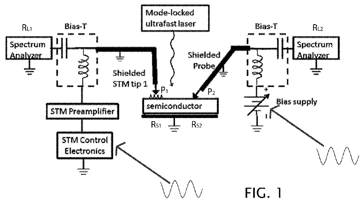
[0019]FIG. 1 is a sketch of one possible implementation of the apparatus for practicing the art of this invention. A STM is provided with control electronics and a preamplifier. The control electronics position a shielded STM tip by operable actuators. The tip (P1) is proximate to, but not touching, a grounded semiconductor sample, thus forming a tunneling junction, while a shielded probe (P2) is positioned on the sample proximate to the tip. A microwave detector, such as a spectrum analyzer (RL2), is also provided in the sample circuit, as is a bias supply. Ideally, but not necessarily, a second microwave detector is provided in the tip circuit, such as the second spectrum analyzer (RL1) in FIG. 1. A...


PUM


Abstract

The superimposition of a periodic potential wave to the tip movement control or the bias supply of an STM, in which a microwave frequency comb is generated in its tunneling junction, may be used to reduce or eliminate artifacts or other noise generated from outside the tunneling junction.

Description

CROSS-REFERENCES TO RELATED APPLICATIONS[0001]This Application claims priority as a non-provisional perfection of prior filed U.S. Application 62 / 474,880, filed Mar. 22, 2017, and incorporates the same by reference in its entirety herein.FIELD OF THE INVENTION[0002]The present invention relates to the field of semiconductor profiling and more particularly relates to the application of a modulating potential to the circuitry of a profiling assembly so as to enable the use of more general mode-locked lasers (active or passive) having an arbitrary carrier frequency and also to enable a greater signal-to-noise ratio.BACKGROUND OF THE INVENTION[0003]The use of a mode-locked ultrafast laser to generate a microwave frequency comb (MFC) in the tunneling junction of a scanning tunneling microscope has been described by this Inventor [M. J. Hagmann, A. J. Taylor and D. A. Yarotski, Observation of 200th harmonic with fractional linewidth of 10−10 in a microwave frequency comb generated in a tu...

Claims


Application Information

Patent Timeline
IPC IPC(8): G01Q30/02G01Q60/12
CPCG01Q30/02G01Q60/12G01Q60/14
Inventor HAGMANN, MARK J.
Owner HAGMANN MARK J
Why Eureka
Try Eureka