
Differential amplification device

a technology of amplification device and amplification device, which is applied in the direction of differential amplifier, amplifier modification to reduce noise influence, amplifier details, etc., can solve the problem of accidental generation of a small output voltage, and achieve the effect of reducing the dc offset voltage and improving the signal-to-noise ratio

Active Publication Date: 2018-10-04
ABLIC INC
View PDF0 Cites 5 Cited by
  • Summary
  • Abstract
  • Description
  • Claims
  • Application Information

AI Technical Summary

Benefits of technology

The present invention provides a differential amplification device that reduces the amplification of the DC offset voltage, resulting in an improved signal-to-noise ratio.

Problems solved by technology

While a zero input voltage means a zero output voltage in an ideal differential amplification device, there are cases in which a slight output voltage is accidentally generated by fluctuations in characteristics and other manufacturing-related factors.

Method used


Image

  • Differential amplification device
  • Differential amplification device
  • Differential amplification device

Examples


first embodiment

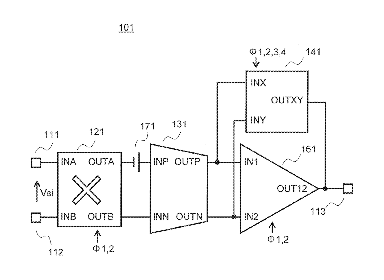
[0022]A first embodiment of the present invention is described below with reference to the drawings. FIG. 1 is a block diagram for illustrating an example of an amplification device according to the first embodiment of the present invention.

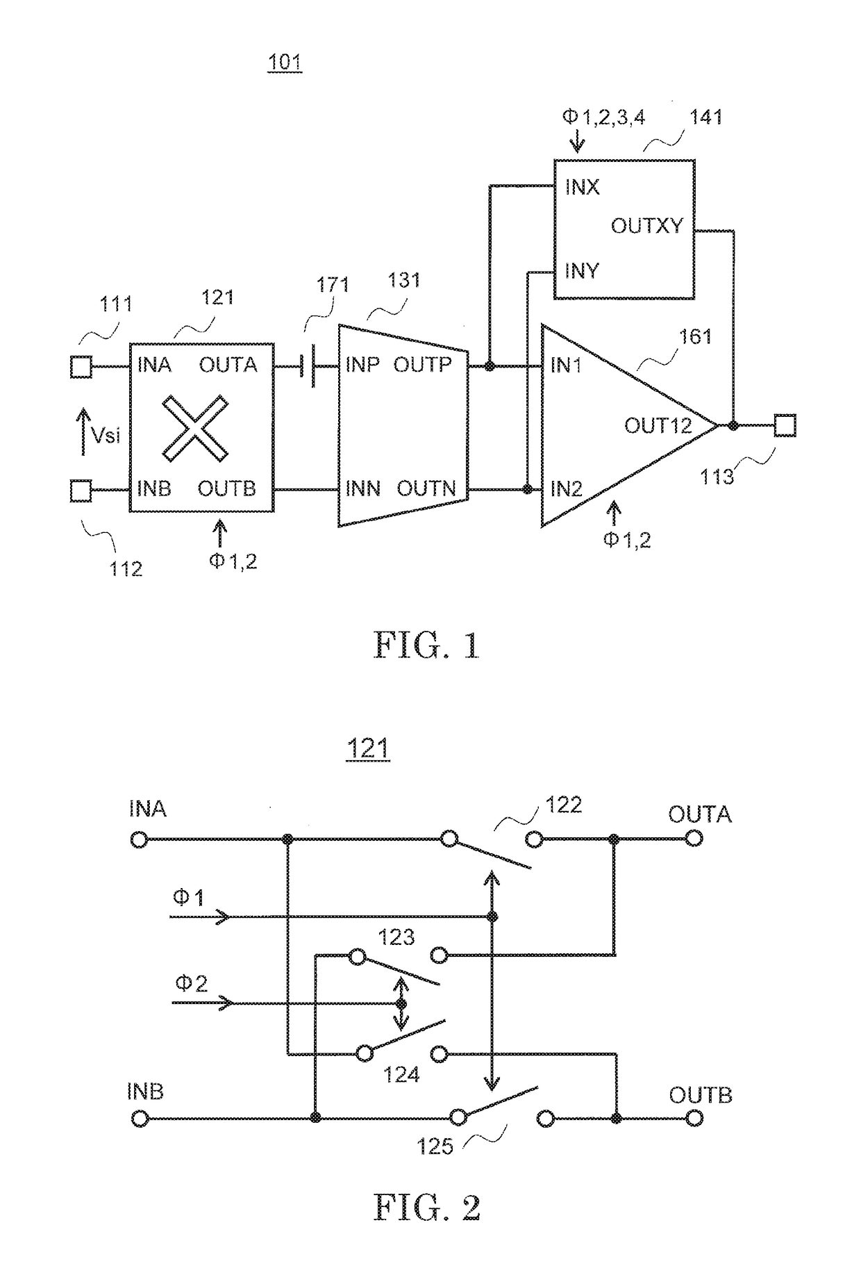
[0023]A differential amplification device 101 according to the first embodiment of the present invention which is illustrated in FIG. 1 includes input terminals 111 and 112, an output terminal 113, a chopper switch circuit 121, a V-I conversion circuit 131, a capacitance circuit 141, and an amplification circuit 161.

[0024]The input terminal 111 is connected to a terminal INA of the chopper switch circuit 121. The input terminal 112 is connected to a terminal INB of the chopper switch circuit 121. A terminal OUTA of the chopper switch circuit 121 is connected to a terminal INP of the V-I conversion circuit 131. A terminal OUTB of the chopper switch circuit 121 is connected to a terminal INN of the V-I conversion circuit 131. The DC offset voltage ...

second embodiment

[0039]A second embodiment of the present invention is described below. The amplification circuit 161 of the first embodiment is an amplification circuit 164 in the second embodiment. FIG. 8 is a diagram for illustrating an example of the configuration of the amplification circuit 164 in the second embodiment. The amplification circuit 164 of FIG. 8 includes terminals IN1, IN2, and OUT12, a differential amplifier 165, a switch 166 switched on / off by the clock signal Φ1, and a switch 167 switched on / off by the clock signal Φ2. The terminal IN1 is connected to an input INP of the differential amplifier 165. The terminal IN2 is connected to an input INN of the differential amplifier 165. The switch 166 switched on / off by the clock signal Φ1 is connected between the terminal OUT12 and OUTP of the differential amplifier 165. The switch 167 switched on / off by the clock signal Φ2 is connected between the terminal OUT12 and OUTN of the differential amplifier 165. The switches 166 and 167 are...

third embodiment

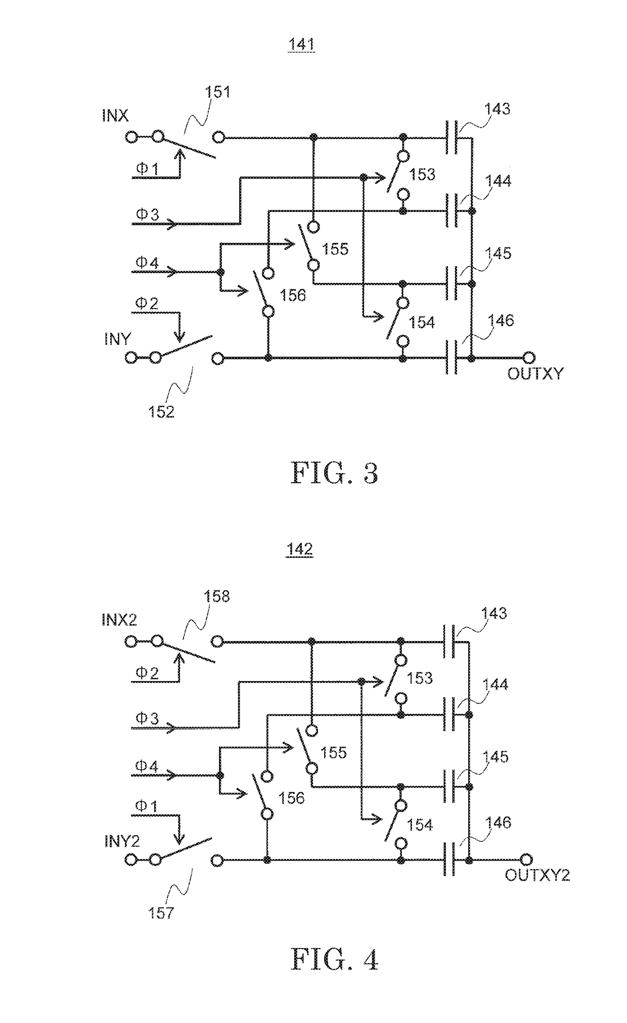
[0041]A third embodiment of the present invention is described below with reference to the drawings. FIG. 9 is a block diagram for illustrating an example of a differential amplification device according to the third embodiment of the present invention. A capacitance circuit 142 which has the same function as that of the capacitance circuit 141, is included in the third embodiment as illustrated in FIG. 9. The capacitance circuit 141 is different from the capacitance circuit 142 in that switches switched on / off by the clock signal Φ1 and switches switched on / off by the clock signal Φ2 are switched with each other. A terminal INX2 of the capacitance circuit 142 is connected to the terminal OUTP of the V-I conversion circuit 131 and the terminal IN1 of the amplification circuit 161. A terminal INY2 of the capacitance circuit 142 is connected to the terminal OUTN of the V-I conversion circuit 131 and the terminal IN2 of the amplification circuit 161. A terminal OUTXY2 of the capacitanc...


PUM


Abstract

Provided is a differential amplification device reduced in DC offset voltage. The amplification device amplifies an input signal, and includes a chopper switch circuit which switches the polarity of the input signal between a normal phase and a reverse phase and outputs the input signal, a V-I conversion circuit which is connected to the chopper switch circuit, a capacitance circuit which is connected to the V-I conversion circuit to store electric charges supplied from the V-I conversion circuit, and an amplification circuit which is connected to the V-I conversion circuit to switch the polarity of an input signal between the normal phase and the reverse phase and amplify the input signal.

Description

RELATED APPLICATIONS[0001]This application claims priority under 35 U.S.C. § 119 to Japanese Patent Application No. 2017-072215 filed on Mar. 31, 2017, the entire content of which is hereby incorporated by reference.BACKGROUND OF THE INVENTION1. Field of the Invention[0002]The present invention relates to a differential amplification device reduced in DC offset voltage.2. Description of the Related Art[0003]Hitherto, it has been known that fluctuations in characteristics among elements cause a DC offset voltage in a differential amplification device. The DC offset voltage refers to a generated non-zero output voltage despite the zero input voltage which is caused by, for example, a short circuit between input terminals of the differential amplification device. While a zero input voltage means a zero output voltage in an ideal differential amplification device, there are cases in which a slight output voltage is accidentally generated by fluctuations in characteristics and other manu...

Claims


Application Information

Patent Timeline
Patent Type & Authority Applications(United States)
IPC IPC(8): H03F1/26H03F3/45
CPCH03F1/26H03F3/45H03F2200/375H03F2200/129H03F2200/372H03F1/303H03F3/45475H03F2203/45551H03F3/387H03F3/45968
Inventor SUGIURA, MASAKAZUTSUZAKI, TOSHIYUKISHIINE, YUJIFUJIMURA, MANABU
Owner ABLIC INC
Learn More