

Heat-sink-attached power-module substrate and power module
- Summary
- Abstract
- Description
- Claims
- Application Information
AI Technical Summary
Benefits of technology
Problems solved by technology
Method used
Image

Examples
examples
[0121]Next, Examples performed for confirming advantageous effects of the present invention will be explained.
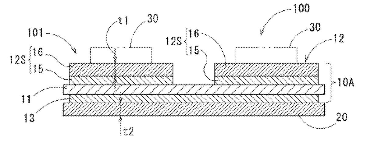
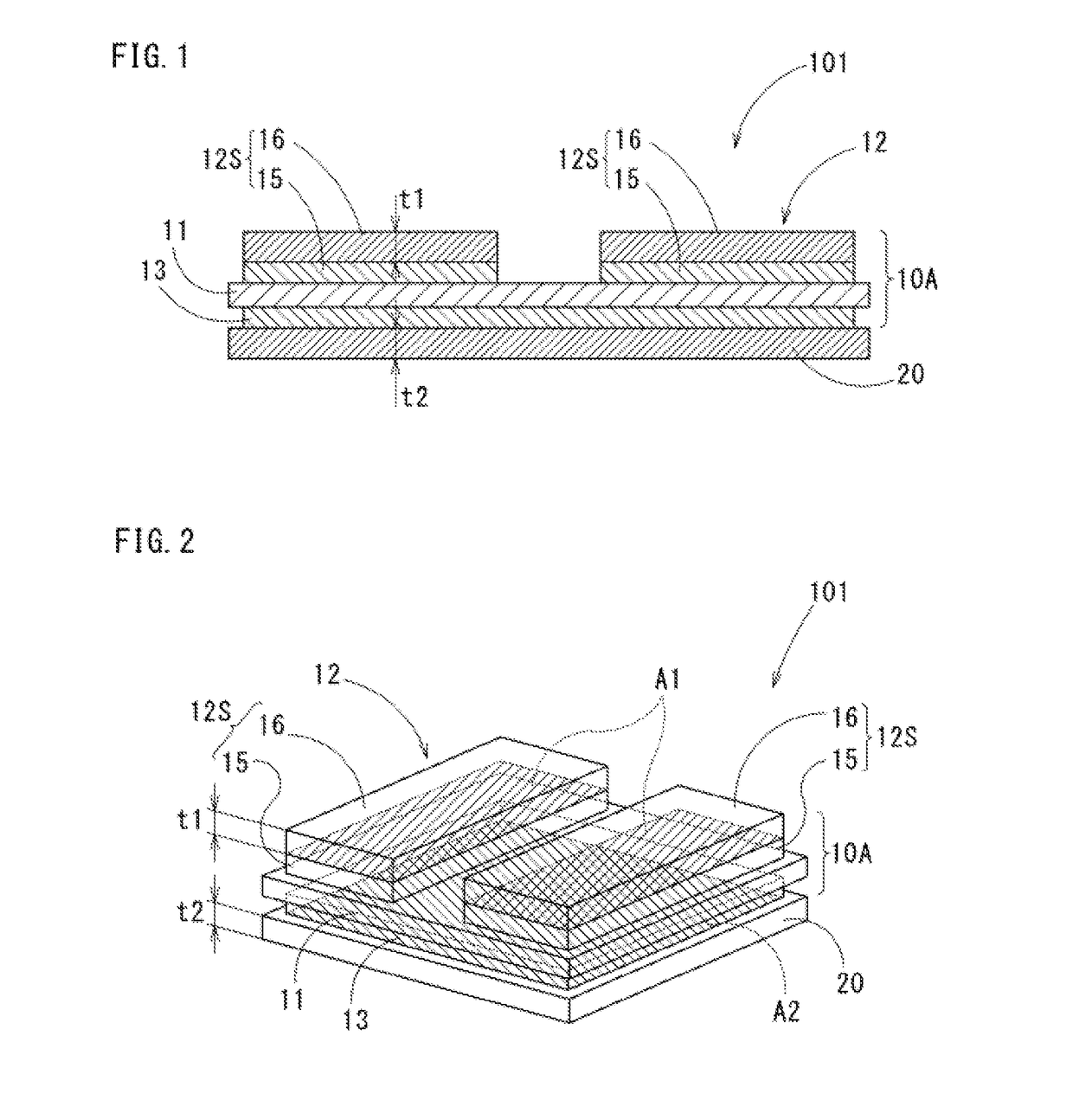
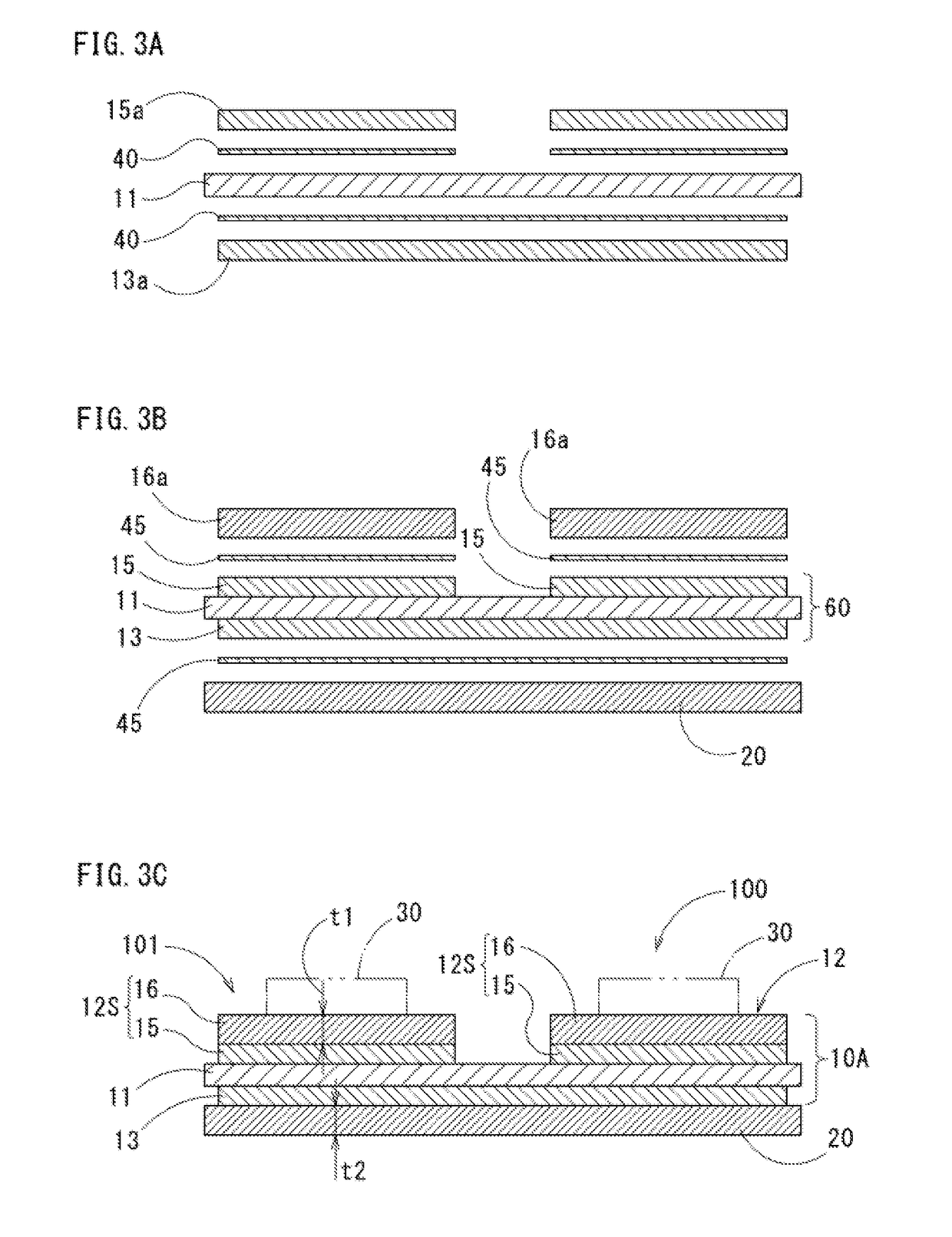
[0122]As Invention Examples 1 to 19, ceramic substrates made of AIN with a thickness of 0.635 mm and first layers and metal layers made of 4N—Al with a thickness of 0.6 mm were prepared: second layers of a circuit layer and heat sinks having thicknesses, joined-surface areas, purities, yield strength shown in Table 1 were prepared.
[0123]The heat sinks had flat plate shape with a plate size of 60 mm×50 mm in all.
[0124]Bonding them by the bonding processes described in the first embodiment to the eighth embodiment, heat-sink-attached power-module substrates were manufactured. Embodiments (bonding methods) in Table 1 show which manufacturing method of the embodiment was applied for manufacturing the respective samples. As Conventional Example 1, a heat-sink-attached power-module substrate was manufactured in which the second layers of the circuit layer were not bonded in the bo...
PUM
| Property | Measurement | Unit |
|---|---|---|
| Temperature | aaaaa | aaaaa |
| Temperature | aaaaa | aaaaa |
| Percent by mass | aaaaa | aaaaa |
Abstract
Description
Claims
Application Information