Solid-state imaging device, manufacturing method thereof, and electronic device
a technology of solid-state imaging and manufacturing methods, applied in semiconductor devices, radio frequency controlled devices, electrical devices, etc., can solve problems such as color mixing, and achieve the effect of improving color mixing and sensitivity
- Summary
- Abstract
- Description
- Claims
- Application Information
AI Technical Summary
Benefits of technology
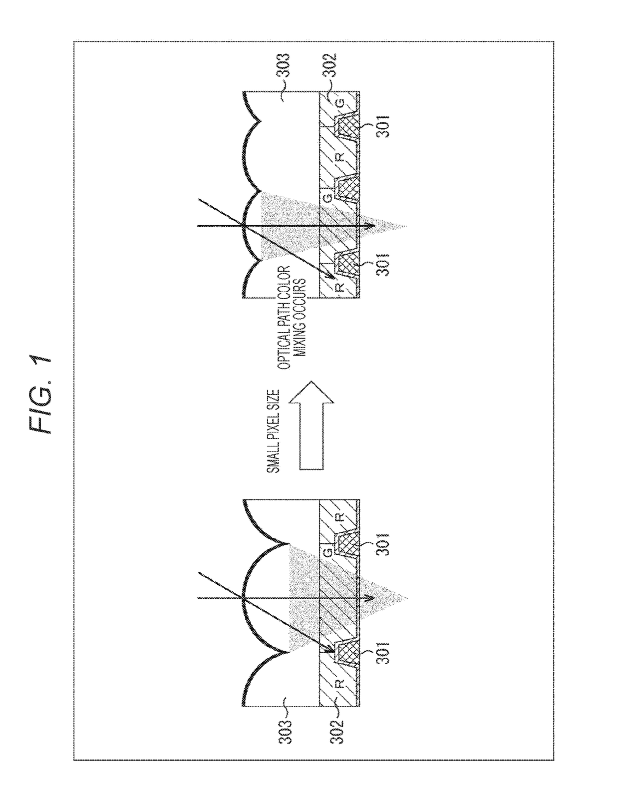
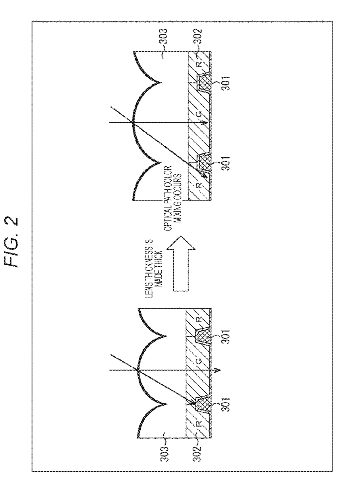
Problems solved by technology
Method used
Image

Examples
first embodiment
[0065]FIG. 5 is a cross-sectional view showing the pixel structure of the first embodiment adopted as the structure of the pixel 2 of the solid-state imaging device 1.
[0066]The semiconductor substrate 12 includes, for example, silicon (Si) and is formed to have a thickness of, for example, 1 to 6 μm. In the semiconductor substrate 12, for example, an N-type (second conductivity type) semiconductor region 42 is formed in a P-type (first conductivity type) semiconductor region 41 for each pixel 2 so that photodiodes PD are formed in units of pixels.
[0067]The upper side of FIG. 5 is the backside of the semiconductor substrate 12 to which light is incident, and the lower side of FIG. 5 is the front side of the semiconductor substrate 12 on which pixel transistors (not shown) and multilayer wiring layers are formed. Therefore, the solid-state imaging device 1 adopting the pixel structure of FIG. 5 is a back-illuminated CMOS image sensor in which light enters from the backside of the semi...
second embodiment
[0095]FIG. 9 is a cross-sectional view showing a pixel structure of a second embodiment adopted as the structure of a pixel 2 of a solid-state imaging device 1.
[0096]In FIG. 9, the parts corresponding to the first embodiment described above are denoted with the same reference numerals, and the description about those parts is omitted as necessary.
[0097]In the second embodiment, on the upper side of a first wall 50, a second wall 100 is further formed so as to separate an on-chip lens 48 of each pixel 2. As shown in FIG. 9, the cross-sectional shape of the second wall 100 is a reverse trapezoid (inverse tapered) shape in which the width of the top where the light enters is the widest and the width becomes thinner toward a semiconductor substrate 12. Alternatively, the cross-sectional shape of the second wall 100 may have a shape in which the top width and the bottom width at the first wall 50 are substantially the same width.
[0098]FIG. 10 shows a relationship between the refractive i...
third embodiment
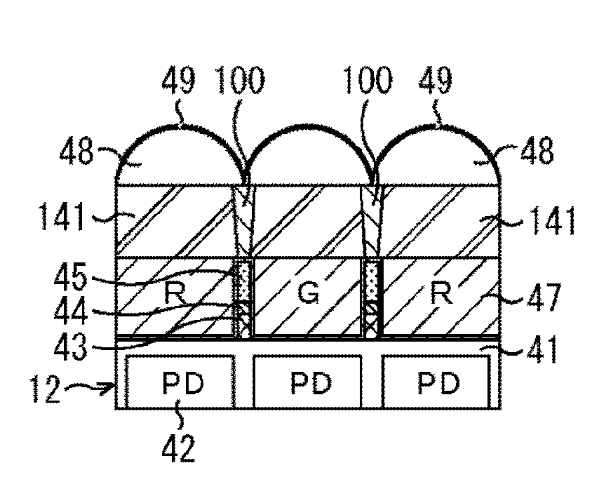
[0119]FIG. 14 is a cross-sectional view showing a pixel structure of a third embodiment adopted as the structure of a pixel 2 of a solid-state imaging device 1.
[0120]In FIG. 14, the parts corresponding to the first and second embodiments described above are denoted with the same reference numerals, and the description about those parts is omitted as necessary.
[0121]In the third embodiment, a second wall 100 is provided on a first wall 50 in a manner similar to the second embodiment shown in FIG. 9. In addition, a high refractive index layer 141 is formed in a region of the same layer region as the second wall 100 on the upper side of a color filter 47. For example, a photosensitive transparent resist or the like having photosensitivity and having a transmittance of 90% or more is used as the material of the high refractive index layer 141. In addition, an on-chip lens 48 and an antireflection film 49 using a material having a still higher refractive index than that of the high refra...
PUM
 Abstract
Description
Claims
Application Information
 - R&D
- Intellectual Property
- Life Sciences
- Materials
- Tech Scout
- Unparalleled Data Quality
- Higher Quality Content
- 60% Fewer Hallucinations
Browse by: Latest US Patents, China's latest patents, Technical Efficacy Thesaurus, Application Domain, Technology Topic, Popular Technical Reports.
© 2025 PatSnap. All rights reserved.Legal|Privacy policy|Modern Slavery Act Transparency Statement|Sitemap|About US| Contact US: help@patsnap.com