Voltage level shifter

a voltage level shifter and voltage level technology, applied in the field of electronic circuits, can solve the problems of power consumption of the voltage level shifter easily becoming too much, and the signal transition speed may also become too slow, so as to reduce the transient current and increase the signal transition speed

Active Publication Date: 2018-10-18
WINBOND ELECTRONICS CORP
View PDF2 Cites 2 Cited by
  • Summary
  • Abstract
  • Description
  • Claims
  • Application Information

AI Technical Summary

Benefits of technology

[0006]In an exemplary embodiment of the invention, the voltage level shifter includes a voltage level shifting circuit and a boost circuit. The voltage level shifting circuit includes a first reference input end, a second reference input end, a first boosted input end, and a second boosted input end. The voltage level shifting circuit operates between a first voltage and a second voltage. The boost circuit is coupled to the voltage level shifting circuit. The boost circuit boosts the first boosted input end and the second boosted input end according to voltage values of the first reference input end and the second reference input end, so as to reduce a transient current that flows from the first voltage to the second voltage.
[0007]According to the above descriptions, in the exemplary embodiments of the invention, the voltage level shifter includes the boost circuit for boosting the first boosted input end and the second boosted input end, so as to reduce the transient current and increase a signal transition speed.

Problems solved by technology

In the conventional art, when the voltage level shifter shifts the voltage signal from a low level to a high level, if a transient current therein is too high, then a power consumption of the voltage level shifter may easily become too much and a signal transition speed may also become too slow.
Therefore, how to provide a voltage level shifter with a low transient current and a fast signal transition speed is an important issue for those technicians of the field.

Method used


Image

  • Voltage level shifter
  • Voltage level shifter

Examples


Embodiment Construction

[0012]Reference will now be made in detail to the present preferred embodiments of the invention, examples of which are illustrated in the accompanying drawings. Wherever possible, the same reference numbers are used in the drawings and the description to refer to the same or like parts.

[0013]The term “coupling / coupled” used in this specification (including claims) of the disclosure may refer to any direct or indirect connection means. In addition, the term “signal” can refer to a current, a voltage, a charge, a temperature, data, electromagnetic wave or any one or multiple signals.

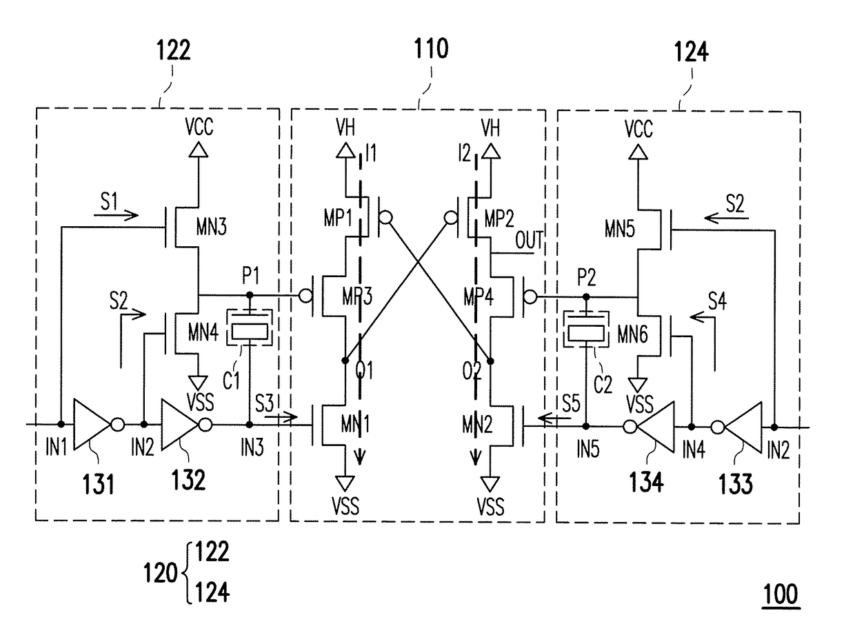
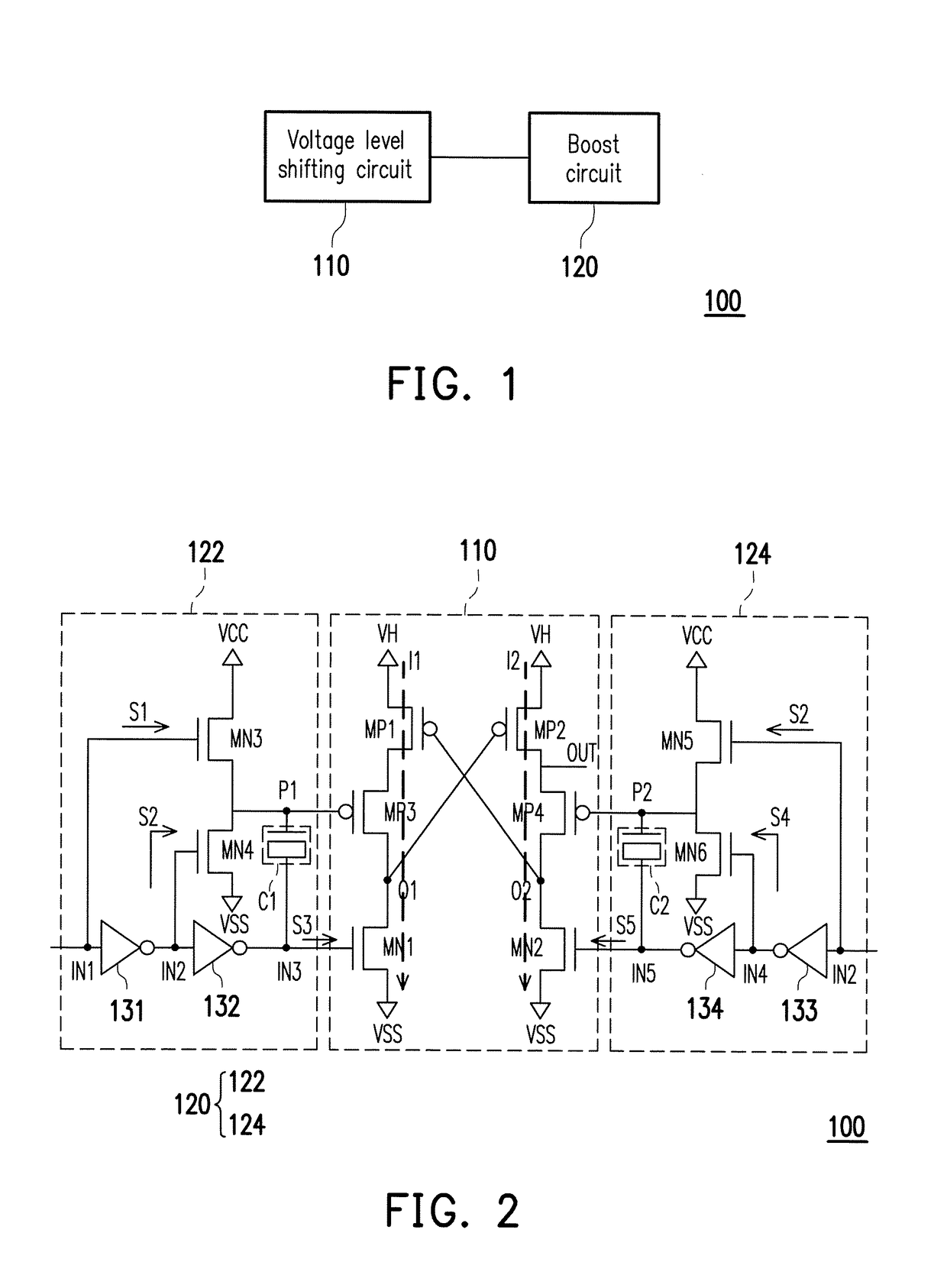
[0014]Referring to FIG. 1 and FIG. 2, a voltage level shifter 100 of the present embodiment includes a voltage level shifting circuit 110 and a boost circuit 120. The boost circuit 120 is coupled to the voltage level shifting circuit 110. In the present embodiment, the voltage level shifting circuit 110 includes a first reference input end IN3, a second reference input end IN5, a first boosted input end P...


PUM


Abstract

A voltage level shifter including a voltage level shifting circuit and a boost circuit is provided. The voltage level shifting circuit includes a first reference input end, a second reference input end, a first boosted input end, and a second boosted input end. The voltage level shifting circuit operates between a first voltage and a second voltage. The boost circuit is coupled to the voltage level shifting circuit. The boost circuit boosts the first boosted input end and the second boosted input end according to voltage values of the first reference input end and the second reference input end to reduce a transient current that flows from the first voltage to the second voltage.

Description

CROSS-REFERENCE TO RELATED APPLICATION[0001]This application claims the priority benefit of China application serial no. 201710238957.3, filed on Apr. 13, 2017. The entirety of the above-mentioned patent application is hereby incorporated by reference herein and made a part of this specification.BACKGROUND OF THE INVENTION1. Field of the Invention[0002]The invention generally relates to an electronic circuit, more particularly, to a voltage level shifter.2. Description of Related Art[0003]With today's rapid development of electronic technology, integrated electronic products having a variety of functions simultaneously have become the focus of market chase. In order to achieve a variety of functions in a single product, switching between different operating voltage ranges is the basic technology required for such product. A protagonist for carrying out the switching between the operating voltage ranges is the so-called voltage level shifter. For example, in a memory storage device, ...

Claims


Application Information

Patent Timeline
Patent Type & Authority Applications(United States)
IPC IPC(8): H03K3/356H03K19/00H02M3/155H03K3/012H03K19/0185
CPCH03K19/018521H02M3/155H03K19/017509
Inventor CHEN, CHUNG-ZEN
Owner WINBOND ELECTRONICS CORP
Why Eureka
Try Eureka