
Luminescent Device

a technology of luminescent devices and t1 host materials, which is applied in the field of organic luminescence technology, can solve the problems of wasting 75% triplet exciton (t1) and seriously restricting the commercial application of pholed

Inactive Publication Date: 2018-10-25
AAC TECH PTE LTD
View PDF0 Cites 4 Cited by
  • Summary
  • Abstract
  • Description
  • Claims
  • Application Information

AI Technical Summary

Benefits of technology

The text suggests that in order to improve the efficiency and performance of OLED displays, particularly those with high current density, a new kind of luminescence mechanism needs to be proposed.

Problems solved by technology

However, the remaining 75% triplet exciton (T1, host material) is wasted due to spin forbidden resistance.
However, the lifetime of phosphorescent OLED (or referred to as PHOLED) and the performance attenuation at high current density are very serious, which seriously limits the further commercial application of PHOLED.

Method used


Image

  • Luminescent Device
  • Luminescent Device
  • Luminescent Device

Examples


Embodiment Construction

[0015]The present disclosure will hereinafter be described in detail with reference to several exemplary embodiments. To make the technical problems to be solved, technical solutions and beneficial effects of the present disclosure more apparent, the present disclosure is described in further detail together with the figure and the embodiments. It should be understood the specific embodiments described hereby is only to explain the disclosure, not intended to limit the disclosure.

[0016]The present disclosure is further elaborated in combination with exemplary embodiments. It should be understood that these embodiments are used only to illustrate the invention and not to limit the scope in the invention.

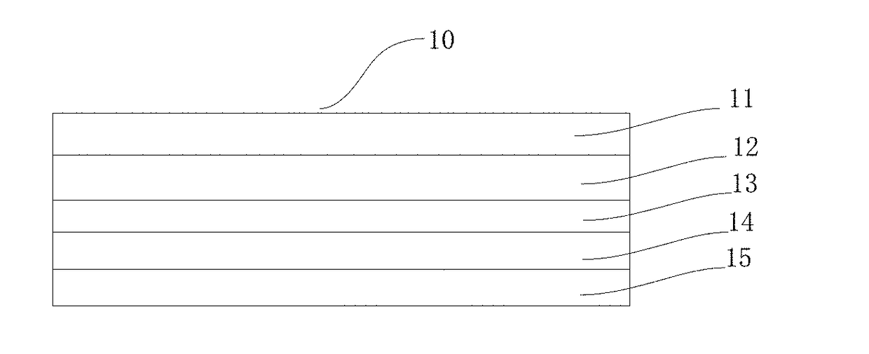
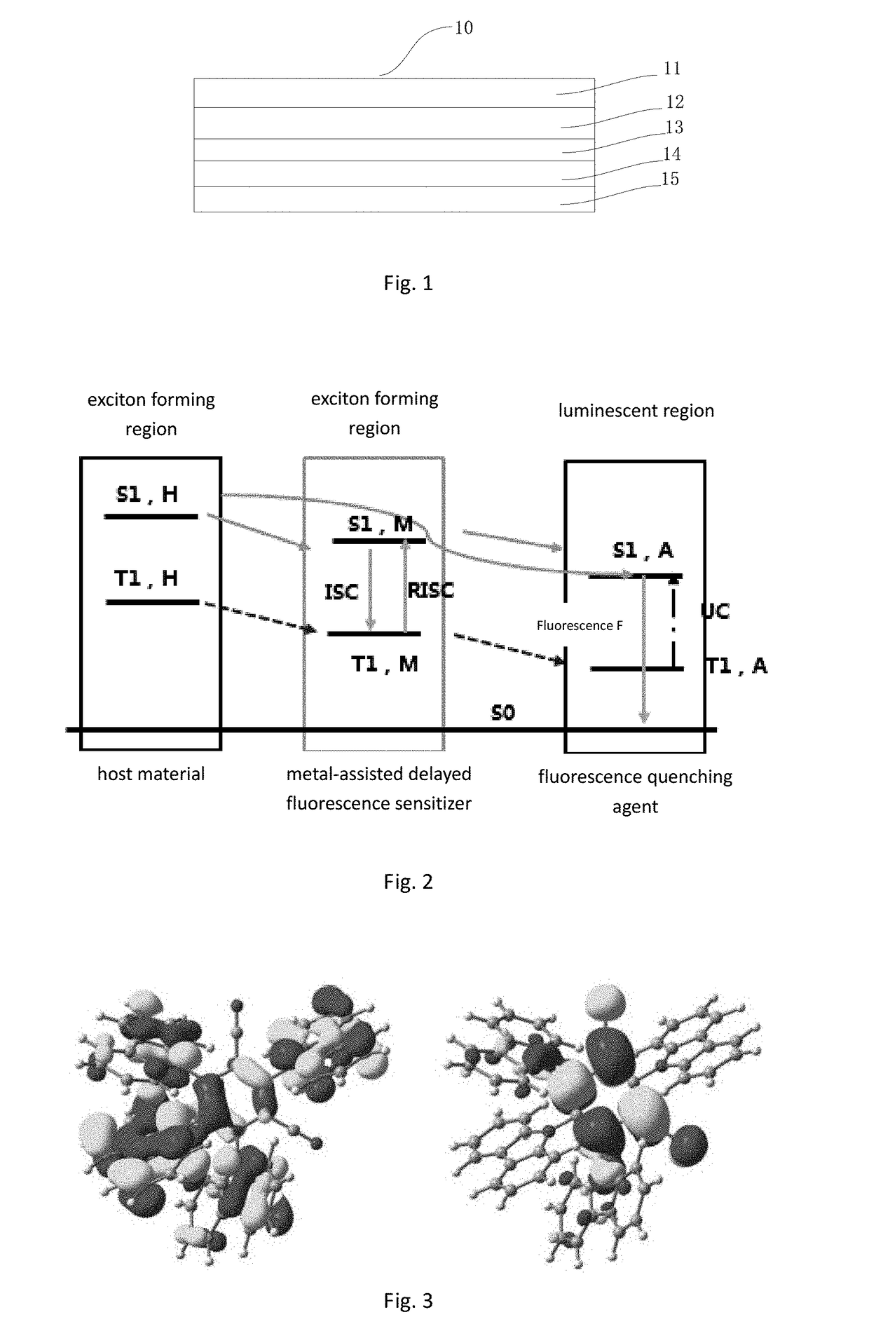
[0017]The invention provides a luminescent device, the structure of which is illustrated in FIG. 1, comprising a first electrode 11, a second electrode 15 and at least an organic luminescent layer 13 arranged between the first electrode 11 and the second electrode 15.

[0018]In the inve...


PUM

PropertyMeasurementUnit
surface roughness Raaaaaaaaaaa
transmittanceaaaaaaaaaa
surface roughness Raaaaaaaaaaa

Abstract

The disclosure relates to organic luminescence technology, in particular to a luminescent device having a first electrode, a second electrode and at least an organic luminescent layer arranged between the first electrode and the second electrode. The organic luminescent layer contains host material, metal-assisted delayed fluorescence sensitizer and fluorescence quenching agent; the metal-assisted delayed fluorescence sensitizer is an organic material which transfers a triplet exciton and a singlet exciton produced by electroluminescence to the fluorescence quenching agent; the fluorescence quenching agent is a fluorescent luminescent material which transfers the energy of all the triplet exciton to the singlet exciton and uses the singlet exciton for luminescence. The luminescent device in the invention has a very high energy utilization rate through the management of exciton in the organic luminescent layer, and significantly improves the luminescent efficiency and service life of the luminescent device.

Description

FIELD OF THE PRESENT DISCLOSURE[0001]The invention relates to the field of organic luminescence technology, in particular to a luminescent device.DESCRIPTION OF RELATED ART[0002]The luminescence mechanism of organic light-emitting diode (OLED) mainly comprises fluorescence and phosphorescence, and the former is mainly a process from singlet excited state to singlet state by using S1→S0, and the latter is mainly a process from triplet excited state to singlet state by using T1→S0. For fluorescent OLED, both holes and electron carriers are injected into the anode and cathode at the same time when the current is driven, and the carriers forms a singlet exciton S1 and three triplet excitons T1 in the host material of the luminescent layer, and then the energy of the singlet exciton S1 of the host material is transferred to the host material's singlet S. Finally, it will be luminescent in the guest material S1→S0. The energy efficiency of this process is relatively low, because, ideally,...

Claims


Application Information

Patent Timeline
Patent Type & Authority Applications(United States)
IPC IPC(8): H01L51/00H01L51/50C07F15/00C09K11/06H10K99/00
CPCH01L51/0084H01L51/5028C07F15/006C09K11/06H01L51/5016H01L51/5056H01L51/5072C09K2211/1029C09K2211/1044C09K2211/185H10K50/12H10K50/11H10K85/626H10K85/615H10K85/341H10K50/121H10K2101/20H10K50/15H10K50/16H10K2101/10
Inventor XIE, ZAIFENG
Owner AAC TECH PTE LTD
Learn More