Connection Panel for Electronic Components

a technology for connecting panels and electronic components, applied in the association of printed circuit non-printed electric components, instruments, fluid speed measurement, etc., can solve the problems of easy damage of flexible foils, laborious stacking of flexible foils, and complicated assembly of acoustically sensitive elements in this acoustic devi

Inactive Publication Date: 2018-10-25
AT & S AUSTRIA TECH & SYSTTECHN AG
View PDF57 Cites 4 Cited by
  • Summary
  • Abstract
  • Description
  • Claims
  • Application Information

AI Technical Summary

Problems solved by technology

In the technical field of printed wiring boards, IC-substrates are known to offer similar functionality in terms of alternately applied conductive and insulating layers, however, IC-substrates are much smaller and often serve to connect a microchip to a printed circuit board.
Assembly of the acoustically sensitive element in this acoustic device is complicated and costly.
Disadvantageously assembly of a stack of flexible foils is labor-intensive while the flexible foils easily can be damaged.
Additionally scale-up of waver-based proce

Method used


Image

  • Connection Panel for Electronic Components
  • Connection Panel for Electronic Components
  • Connection Panel for Electronic Components

Examples


Embodiment Construction

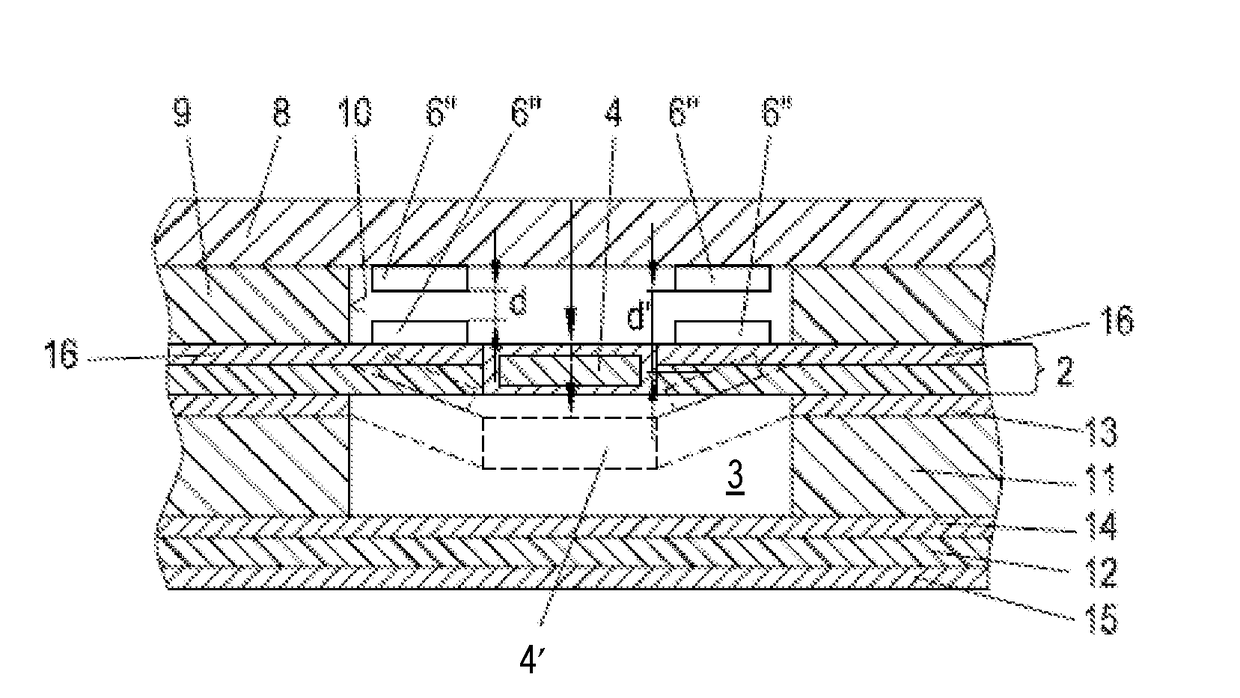
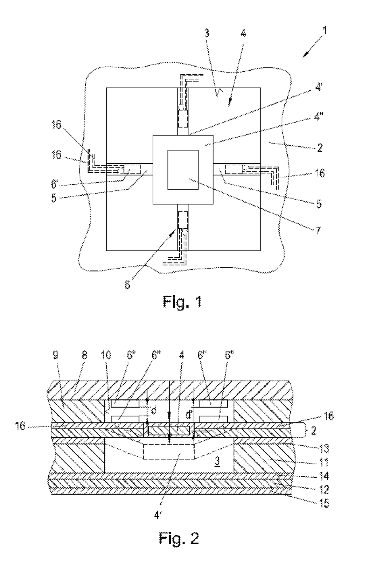
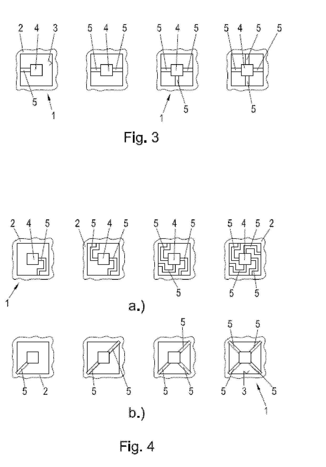
[0009]In particular the invention provides for a connection panel for electronic components of the initially mentioned kind which is characterized in that the sensor is comprised of at least one flexure member formed by a flexure layer, the flexure member protruding from the flexure layer and into a clearance within the flexure layer and carrying at least a part of a flexure sensing device. The flexure layer usually is formed by one insulating layer but it can also be comprised of a plurality of insulating layers and conductive layers. For the purposes of this description and the appended claim, the flexure layer is defined as a layer having a clearance to form the flexure member as a part of the flexure layer reaching into the clearance, thus being more prone to flexing, vibrating and / or to being depressed by pressure than the remainder of the flexure layer. The clearance can be a simple cut having a deflection so that the minimum configuration of the flexure member is that of a to...


PUM


Abstract

In a connection panel for electronic components comprising a plurality of insulating layers and conductive layers and further comprising an electronic sensor, the sensor is comprised of at least one flexure member formed by a flexure layer, the flexure member protruding from the flexure layer and into a clearance within the flexure layer and carrying at least a part of a flexure sensing device.

Description

[0001]The invention relates to a connection panel for electronic components comprising a plurality of insulating layers and conductive layers and further comprising an electronic sensor as well as the use thereof.DESCRIPTION OF THE RELATED ART[0002]The invention relates to connection panels for electronic components in general, wherein electronic components such as transistors, integrated circuits (ICs, microchips) and the like are arranged on or embedded within a panel carrying and electrically connecting those electronic components. Such connection panels can be printed circuit boards (PCBs) or IC-substrates used for connecting a single integrated circuit or a plurality of integrated circuits to a printed circuit board. In fact, IC-substrates and printed circuit boards are highly similar in their basic functionalities and differ merely in size as will be explained and defined at a later stage of this description. For the purposes of this description the terms “printed circuit boar...

Claims


Application Information

Patent Timeline
IPC IPC(8): H05K1/18B81B7/00H01L41/053H01L41/113G01P1/02G01L1/22
CPCB81B2201/0264B81B2203/0109B81B2207/07B81B2203/0315H05K2201/10151G01L1/148G01L1/12G01L1/16G01P15/00G01L1/2262H05K2201/10083H05K1/185B81B7/0006H01L41/053H01L41/1132G01P1/023G01L1/2293B81B2201/0235B81B2203/0163B81C1/00142B81B2201/0257B81B2203/053H05K1/162H10N30/88H10N30/302
Inventor KASPER, ALEXANDERGRABMAIER, SANDRALEITGEB, MARKUS
Owner AT & S AUSTRIA TECH & SYSTTECHN AG
Why Eureka
Try Eureka