Chip scale optical systems

a technology of optical systems and chips, applied in the field of optical phased arrays, can solve the problems of affecting the range of practical applications, and affecting the operation of optical systems

Inactive Publication Date: 2018-11-08
CHARLES STARK DRAPER LABORATORY
View PDF0 Cites 13 Cited by
  • Summary
  • Abstract
  • Description
  • Claims
  • Application Information

AI Technical Summary

Benefits of technology

[0014]In one or more embodiments, the optical phased array of these teachings includes a wafer, a plurality of optical waveguides; the plurality of optical waveguides being one of implanted in the wafer or disposed on the wafer; a root optical waveguide, the root optical waveguide being one of implanted in the wafer or disposed on the wafer, the root optical waveguide being optically connected at one end to one optical waveguide from the plurality of optical waveguides, another end of the root optical waveguide constituting an optical port, a plurality of optical couplers disposed in an array and located on the wafer, the plurality of optical waveguides optically connecting the plurality of optical couplers to the optical port via respective optical paths, one optical path per optical coupler, and a plurality of configurable optical delay lines; each configurable optical delay line from the plurality of configurable optical delay lines being disposed in one respective optical path from the respective optical paths; the plurality of configurable optical delay lines being configured such that the plurality of optical couplers emit a non-planar phase front near field radiation pattern, the plurality of optical couplers receiving light from a light source coupled to the optical port.

Problems solved by technology

Signals radiated by the various antennas constructively and destructively interfere with each other in the space in front of the antenna array.
In many of those applications, the range of practical applications is hindered by the size of the optical system.
A common limitation in microscopy applications is the inability to image deep within tissue or turbid / strongly scattering media.
Index variations lead to scattering and the distortion of phase fronts, which impact imaging mechanisms and reduce signal.
This can limit the effectiveness of confocal microscopy, fluorescence microscopy, and two-photon microscopy or place limitations on the thickness of samples investigated with these techniques because all three rely on achieving a tightly focused beam spot at the focal point.
However, phase conjugate imaging often relies on free space optics, precise alignment, and requiring the use of an SLM greatly increases the cost of the equipment.

Method used


Image

  • Chip scale optical systems
  • Chip scale optical systems
  • Chip scale optical systems

Examples


Embodiment Construction

[0036]The description is not to be taken in a limiting sense, but is made merely for the purpose of illustrating the general principles of these teachings, since the scope of these teachings is best defined by the appended claims.

[0037]The above illustrative and further embodiments are described below in conjunction with the following drawings, where specifically numbered components are described and will be appreciated to be thus described in all figures of the disclosure:

[0038]As used herein, the singular forms “a,”“an,” and “the” include the plural reference unless the context clearly dictates otherwise.

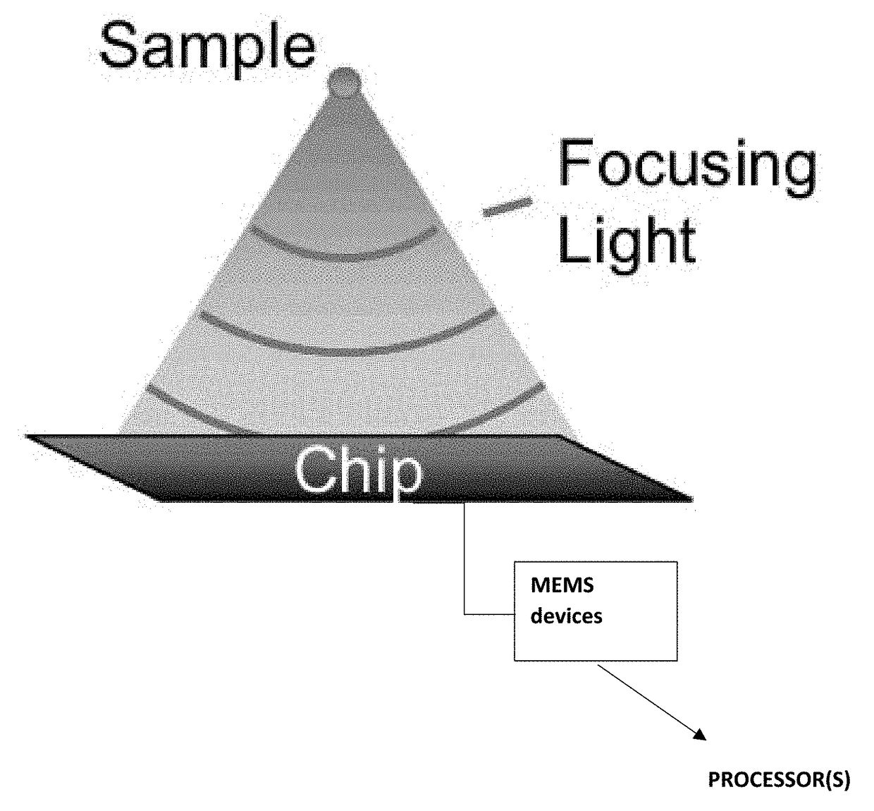
[0039]Embodiments of optical system reduced to the size of the chip are disclosed herein below.

[0040]In order to elucidate these teachings, two related systems are presented herein below.

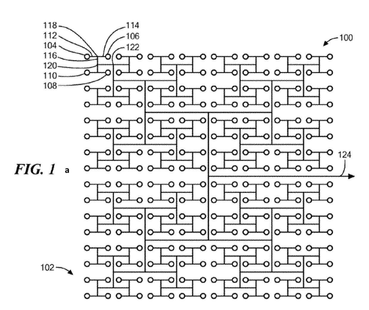
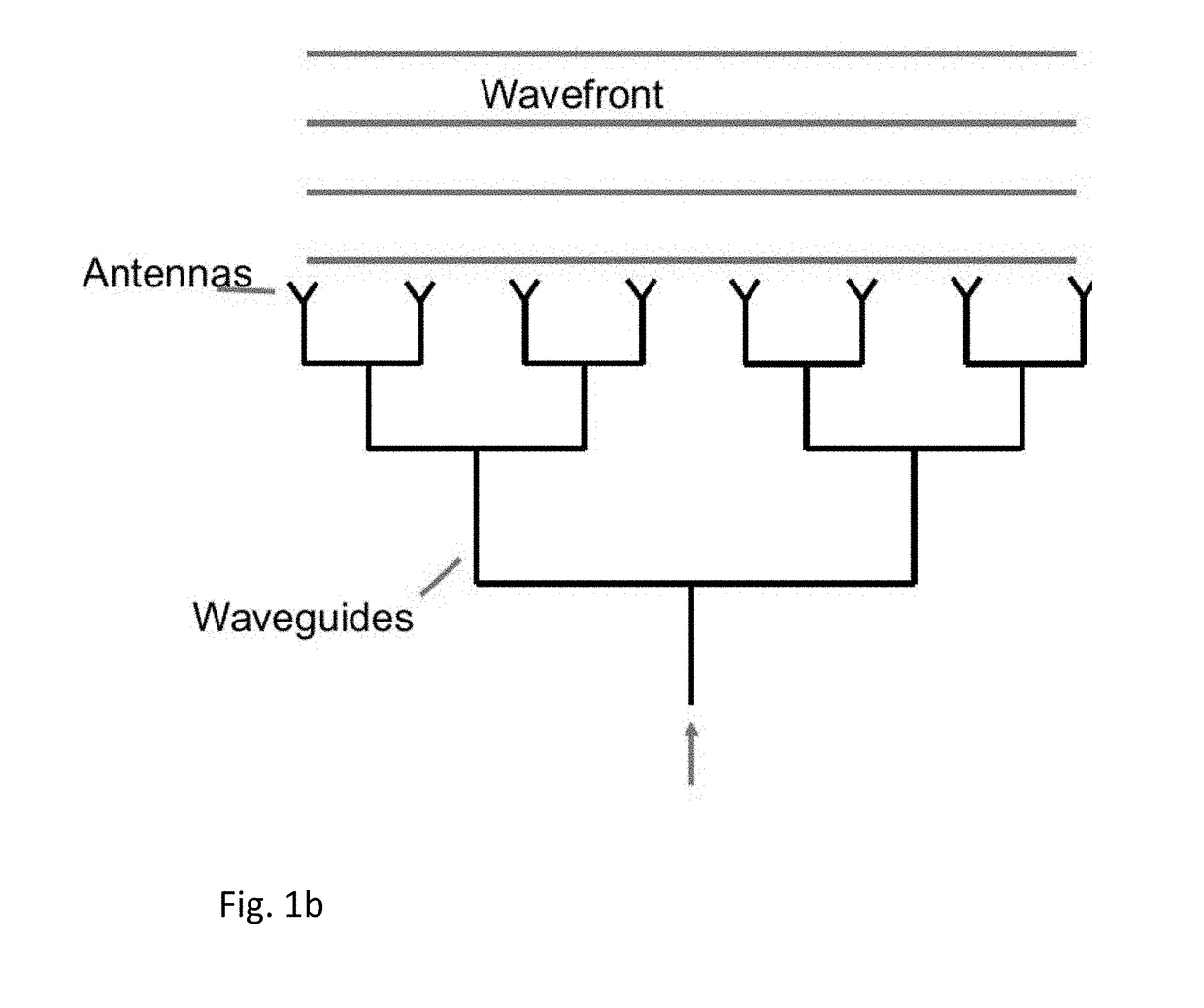
[0041]Sun, Watts, et al., describe a phased array of optical antennas. (See U.S. Pat. No. 8,988,754 and Sun, Watts, et al., “Large-scale nanophotonic phased array,” Nature, Vol. 493, pp. 195-199, ...


PUM

PropertyMeasurementUnit
optical pathaaaaaaaaaa
optical pathsaaaaaaaaaa
confocal microscopeaaaaaaaaaa

Abstract

An optical phased array including a wafer, optical waveguides, a root optical waveguide, the root optical waveguide being optically connected at one end to one optical waveguide, another end of the root optical waveguide constituting an optical port, optical couplers disposed in an array and located on the wafer, the optical waveguides optically connecting the optical couplers to the optical port via respective optical paths, one optical path per optical coupler, configurable optical delay lines; each configurable optical delay line being disposed in one respective optical path from the respective optical paths; the configurable optical delay lines being configured such that the optical couplers emit a non-planar phase front near field radiation pattern from light received from a light source coupled to the optical port.

Description

CROSS REFERENCE TO RELATED APPLICATIONS[0001]This application claims priority to and benefit of U.S. Provisional Application No. 62 / 501,389, filed May 4, 2017, entitled CHIP SCALE OPTICAL SYSTEMS, which is incorporated by reference herein in its entirety for all purposes.BACKGROUND[0002]This invention relates generally to optical phased arrays and, more particularly, to optical components including optical phased arrays.[0003]Phased arrays of antennas are used in radar and other applications in which a direction of an incoming radio frequency (RF) signal needs to be ascertained or in which an RF signal needs to be transmitted in a particular direction. One or more receivers, transmitters or transceivers are electrically connected to an array of antennas via feed lines, such as waveguides or coaxial cables. Taking a transmitter case as an example, the transmitter(s) operate such that the phase of the signal at each antenna is separately controlled. Signals radiated by the various ant...

Claims


Application Information

Patent Timeline
Patent Type & Authority Applications(United States)
IPC IPC(8): G02F1/21G02F1/295G02B6/12G02B6/35G02F1/125
CPCG02F1/218G02F1/2955G02B6/12033G02B6/3546G02B6/12011G02F1/125G01N21/4795G02B21/0032G02B21/0056G02B21/0076G02B27/58
Inventor SPECTOR, STEVENDAWSON, ROBINLANE, BENJAMINMOEBIUS, MICHAEL G.
Owner CHARLES STARK DRAPER LABORATORY
Why Eureka
Try Eureka