Methods for selectively forming a silicon nitride film on a substrate and related semiconductor device structures

a technology of silicon nitride and substrate, which is applied in the direction of semiconductor/solid-state device details, coatings, chemical vapor deposition coatings, etc., can solve the problems of device integration, device performance degradation, and limited deposition performance of plasma based deposition processes

Active Publication Date: 2018-11-08
ASM IP HLDG BV
View PDF9 Cites 265 Cited by
  • Summary
  • Abstract
  • Description
  • Claims
  • Application Information

AI Technical Summary

Benefits of technology

[0008]In accordance with at least one embodiment of the disclosure, a method for selectively forming a silicon nitride film a on substrate comprising a first metallic surface and a second dielectric surface by a cyclical deposition process is provided. The method may comprise, contacting the substrate with a first reactant comprising a silicon halide source, contacting the substrate with a second reactant comprising a nitrogen source, wherein the incubation delay for the first metallic surface is less than the incubation delay for the second dielectric surface.

Problems solved by technology

State of the art device structures may not be able to withstand such a high thermal budget which may further result in a deterioration of device performance and may cause device integration problems.
However, plasma based deposition processes may be limited in deposition performance, i.e., step coverage, uniformity of film quality achievable for high aspect ratio structures and plasma based deposition processes may damage the underlying device structures.
Such processing is time consuming and expensive, and does not offer the precision required for many applications.

Method used


Image

  • Methods for selectively forming a silicon nitride film on a substrate and related semiconductor device structures
  • Methods for selectively forming a silicon nitride film on a substrate and related semiconductor device structures
  • Methods for selectively forming a silicon nitride film on a substrate and related semiconductor device structures

Examples


Embodiment Construction

[0016]Although certain embodiments and examples are disclosed below, it will be understood by those in the art that the invention extends beyond the specifically disclosed embodiments and / or uses of the invention and obvious modifications and equivalents thereof. Thus, it is intended that the scope of the invention disclosed should not be limited by the particular disclosed embodiments described below.

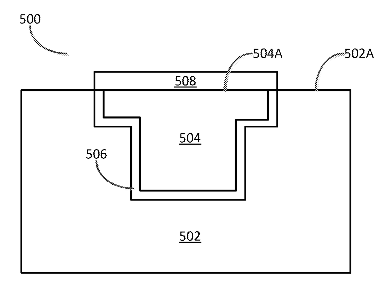
[0017]As used herein, the term “metallic surface” may refer to a surface including metal ions and may further include, but is not limited to, metals, metal alloys, metal salts, metal oxides, metal silicides, metal borides, semi-metals and metal nitrides.

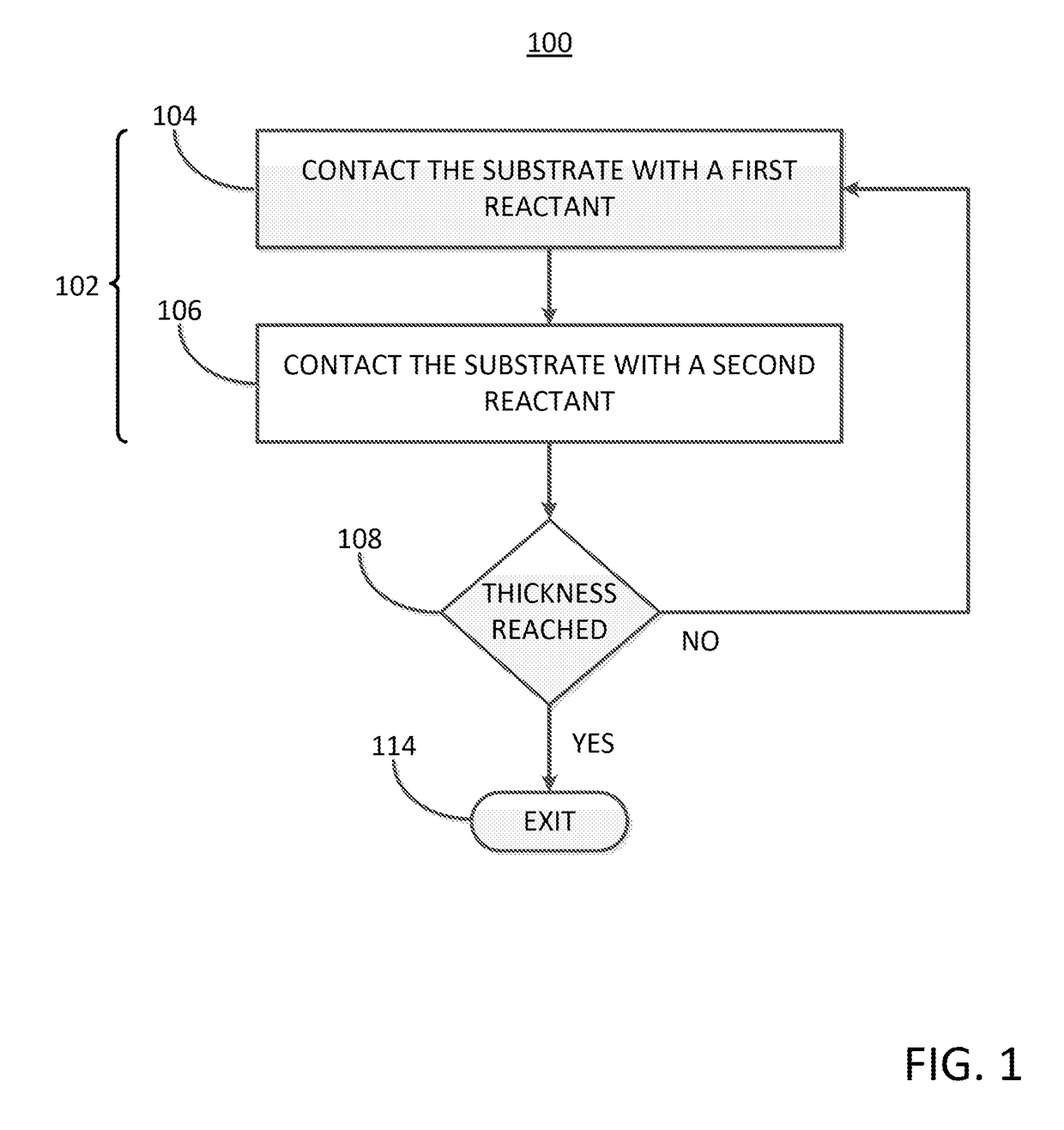
[0018]As used herein, the term “cyclic deposition” may refer to the sequential introduction of precursors (reactants) into a reaction chamber to deposit a layer over a substrate and includes processing techniques such as atomic layer deposition and cyclical chemical vapor deposition.

[0019]As used herein, the term “incubation period” may...


PUM

PropertyMeasurementUnit
temperatureaaaaaaaaaa

Abstract

A method for selectively forming a silicon nitride film on a substrate comprising a first metallic surface and a second dielectric surface by a cyclical deposition process is disclosed. The method may comprise contacting the substrate with a first reactant comprising a silicon halide source and contacting the substrate with a second reactant comprising a nitrogen source, wherein the incubation period for the first metallic surface is less than the incubation period for the second dielectric surface. Semiconductor device structures comprising a selective silicon nitride film are also disclosed.

Description

FIELD OF INVENTION[0001]The present disclosure generally relates to methods for selectively forming a silicon nitride film on a substrate and related semiconductor device structures including a selective silicon nitride film.BACKGROUND OF THE DISCLOSURE[0002]In the field of semiconductor device technology silicon nitride films may be utilized during the fabrication of semiconductor integrated circuitry. For example, silicon nitride films may be utilized as an insulating material during the fabrication of semiconductor device structures, such as, for example, transistors, memory cells, logic devices, memory arrays, etc.[0003]There is a need in the field of semiconductor device technology for low temperature deposition processes for high quality silicon nitride films; such low temperature deposition processes should also provide precise control of the film thickness, thickness uniformity and conformality.[0004]Common silicon nitride film deposition processes require high temperature d...

Claims


Application Information

Patent Timeline
Patent Type & Authority Applications(United States)
IPC IPC(8): H01L21/02H01L21/311H01L21/768C23C16/34C23C16/455C23C16/56
CPCH01L21/0228H01L21/0217H01L21/31116C23C16/56C23C16/345C23C16/45553H01L21/76834C23C16/04H01L21/02211H01L21/0254H01L21/02532H01L21/324H01L21/02208H01L23/00
Inventor WOODRUFF, JACOB HUFFMANSHARMA, BED
Owner ASM IP HLDG BV
Why Eureka
Try Eureka