Organic light emitting diode assembly, manufacturing method thereof, and display panel

a technology of light-emitting diodes and assembly, which is applied in the direction of organic semiconductor devices, solid-state devices, semiconductor devices, etc., can solve the problems of poor stability, short life, low color gamut, etc., and achieves the effects of improving the stability of the electrode, prolonging the life of the oled device, and low chemical activity

Inactive Publication Date: 2018-11-08
TCL CHINA STAR OPTOELECTRONICS TECH CO LTD
View PDF10 Cites 1 Cited by
  • Summary
  • Abstract
  • Description
  • Claims
  • Application Information

AI Technical Summary

Benefits of technology

[0003]The present invention mainly provides an organic light emitting display assembly, a manufacturing thereof, and a display panel to the technical problem, it can improve the color gamut and stability of OLED devices, and extend the life of OLED devices.
[0007]The present invention can be concluded with the following advantages, the OLED assembly provided by the present invention is different from the prior art that the OLED assembly selects a metal layer with a high-power function as the anode layer, these metals with a high-power function have low chemical activity, can improve the stability of the electrode, thereby extending the life of OLED devices. In addition, the electron transport layer of the OLED assembly is doped with a quantum dot material, and the emission spectrum of the quantum dot light emitting material is concentrated, and the color purity is high, and the color gamut of the OLED display can be improved.

Problems solved by technology

The inventor of the present invention has found that the OLED device in the prior art has problems that the color gamut is low, the stability is poor, and the lifetime is short.

Method used


Image

  • Organic light emitting diode assembly, manufacturing method thereof, and display panel
  • Organic light emitting diode assembly, manufacturing method thereof, and display panel
  • Organic light emitting diode assembly, manufacturing method thereof, and display panel

Examples


Embodiment Construction

[0012]Technical implementation will be described below clearly and fully by combining with drawings made in accordance with an embodiment in the present invention.

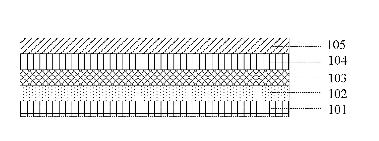
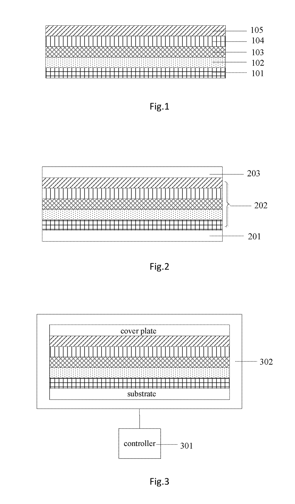
[0013]Referring to FIG. 1, FIG. 1 is a structural illustration of an embodiment in accordance to an organic light emitting assembly in the present invention. The OLED assembly of the embodiment comprises an anode layer 105, an electron hole transport layer 104, a light emitting layer 103, an electron transport layer 102, and a cathode layer 101 arranged sequentially, wherein the anode layer 105 is a metal layer with a high-power function, and the electron transport layer 102 comprises a quantum dot material.

[0014]OLED display driver is divided into passive matrix driving (PM-OLED) and active matrix driving (AM-OLED); active matrix driving is divided into amorphous silicon thin film transistor (a-Si TFT) technology and low temperature polysilicon thin film transistor (LTPS TFT) technology; and TFT is divided into p-type TFT...


PUM


Abstract

The present invention mainly provides an organic light emitting display assembly, a manufacturing thereof, and a display panel. The organic light emitting diode assembly comprises an anode layer, an electron hole transport layer, a light emitting layer, an electron transport layer, and a cathode layer arranged sequentially, wherein the anode layer is a metal layer with a high-power function, and the electron transport layer comprises a quantum dot material. By the above-mentioned method, the present invention can improve the stability of the electrode, thereby extending the life of OLED devices, and the color gamut of the OLED display can be improved.

Description

FIELD OF THE INVENTION[0001]The present invention relates to a technology of organic light emitting display panel, and more particularly, to an organic light emitting display assembly, manufacturing thereof, and display panel.DESCRIPTION OF PRIOR ART[0002]Organic Light Emitting Diodes (OLED) as a new generation of flat panel display devices, with advantages such as self-luminous, wide viewing angle, high contrast, fast response, low power consumption, is expected to become the next generation of mainstream flat panel display technology, and is one of the most watched technologies in flat panel display technology. The inventor of the present invention has found that the OLED device in the prior art has problems that the color gamut is low, the stability is poor, and the lifetime is short.SUMMARY OF THE INVENTION[0003]The present invention mainly provides an organic light emitting display assembly, a manufacturing thereof, and a display panel to the technical problem, it can improve t...

Claims


Application Information

Patent Timeline
Patent Type & Authority Applications(United States)
IPC IPC(8): H01L51/50H01L51/56H01L51/52
CPCH01L51/5076H01L51/56H01L51/5206H01L2251/5369H01L51/0005H01L51/0021H01L2251/5353H10K71/135H10K71/164H10K50/16H10K2102/331H10K50/165H10K50/81H10K71/00H10K71/60H10K2102/321
Inventor ZHANG, YUNANSHI, TING
Owner TCL CHINA STAR OPTOELECTRONICS TECH CO LTD
Why Eureka
Try Eureka