Wafer processing method

Active Publication Date: 2018-11-15
DISCO CORP
View PDF0 Cites 1 Cited by
  • Summary
  • Abstract
  • Description
  • Claims
  • Application Information

AI Technical Summary

Benefits of technology

The present invention provides a wafer processing method that can effectively suppress the influence of asperities on the front side of the wafer and simplify the peeling operation after grinding. This method includes steps of close contact making, covering with a protective member, grinding the back side of the wafer, and peeling the protective member and protective film from the wafer. The method effectively absorbs the asperities on the front side of the wafer and eliminates the need for extensive work to peel the protective film.

Problems solved by technology

In many cases, asperities such as bumps functioning as electrodes on each device are formed on the front side of the wafer.
However, when such asperities are present on the front side of the wafer, there arises a problem such that a height difference due to the asperities cannot be sufficiently absorbed by an adhesive tape and the shape corresponding to each asperity may appear on the back side of the wafer after grinding.

Method used


Image

  • Wafer processing method
  • Wafer processing method
  • Wafer processing method

Examples


Embodiment Construction

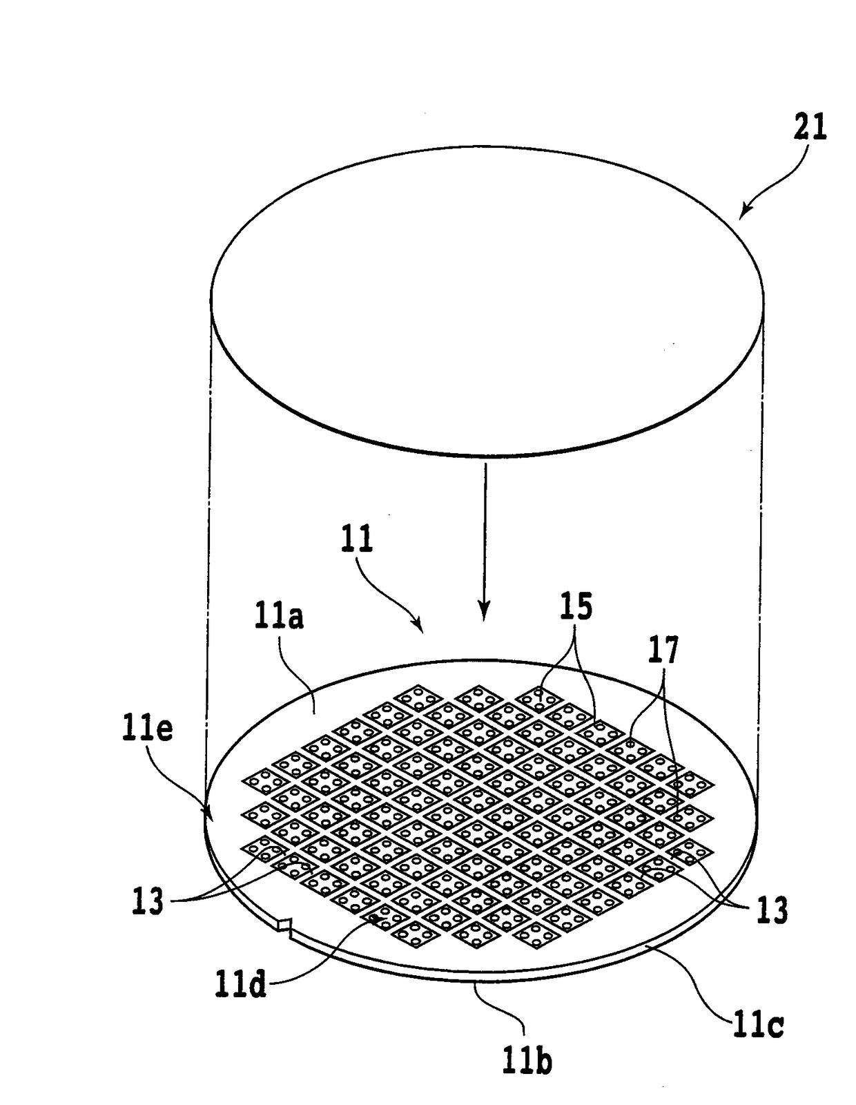
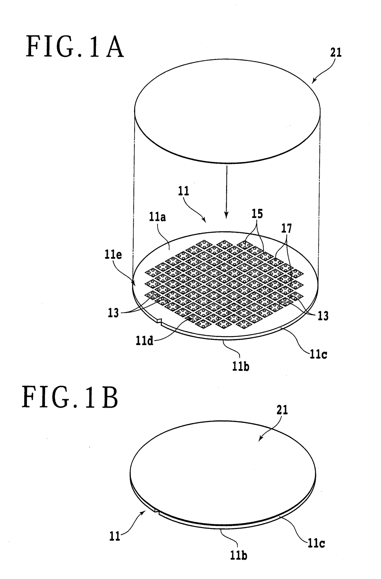
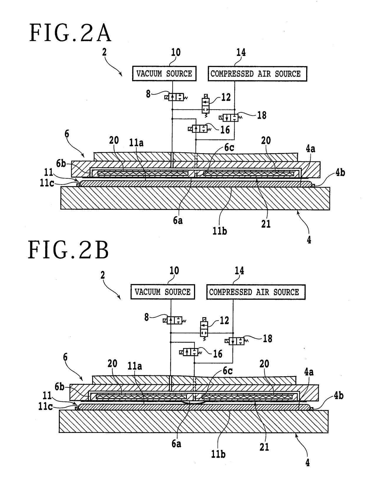
[0038]A preferred embodiment of the present invention will now be described with reference to the attached drawings. The wafer processing method according to this preferred embodiment includes a close contact making step (see FIGS. 1A, 1B, 2A, 2B, 3A, and 3B), a protective member fixing step (see FIGS. 4A, 4B, and 4C), a grinding step (see FIGS. 5A and 5B), and a peeling step (see FIG. 6). In the close contact making step, a protective film not having adhesion by an adhesive (paste) is brought into close contact with the front side of a wafer so as to follow asperities formed on the front side of the wafer. In the protective member fixing step, the protective film is covered with a protective member formed from a liquid resin to thereby fix the protective member through the protective film to the front side of the wafer. In the grinding step, the back side of the wafer is ground in the condition where the protective member fixed through the protective film to the front side of the w...


PUM


Abstract

A wafer processing method includes a close contact making step of pressing a protective film against the front side of a wafer in a radially outward direction starting from the center of the wafer to thereby bring the protective film into close contact with the front side of the wafer, a protective member fixing step of covering the protective film with a protective member formed by curing a liquid resin to thereby fix the protective member through the protective film to the front side of the wafer, a grinding step of grinding the back side of the wafer to reduce the thickness of the wafer, and a peeling step of peeling the protective film and the protective member from the wafer thinned by the grinding step.

Description

BACKGROUND OF THE INVENTIONField of the Invention[0001]The present invention relates to a wafer processing method for use in grinding a wafer having asperities formed on the front side.Description of the Related Art[0002]There is an increasing chance of thinning a wafer before dividing the wafer into device chips, so as to reduce the size and weight of each device chip adapted to be incorporated into various electronic equipment or the like. For example, the wafer can be thinned by holding the front side of the wafer on which devices are formed on a chuck table, rotating a grinding wheel, and pressing the grinding wheel against the back side of the wafer to thereby grind the back side of the wafer.[0003]In grinding the wafer by using the above method, a protective member is usually attached to the front side of the wafer (see Japanese Patent Laid-Open No. Hei 10-50642, for example). The protective member can prevent the possibility that the devices formed on the front side of the wa...

Claims


Application Information

Patent Timeline
IPC IPC(8): H01L21/02B24B7/22
CPCH01L21/02013H01L21/02016B24B7/228H01L21/6836H01L2221/68386H01L2221/6834H01L2221/68327H01L21/67092H01L21/67132H01L21/6838
Inventor SEKIYA, KAZUMA
Owner DISCO CORP
Why Eureka
Try Eureka