Circuitry and methods for programming resistive random access memory devices

a random access memory and circuit technology, applied in semiconductor devices, digital storage, instruments, etc., can solve problems such as limiting the capacitive dump spike curren

Active Publication Date: 2019-02-14
MICROSEMI SOC
View PDF0 Cites 13 Cited by
  • Summary
  • Abstract
  • Description
  • Claims
  • Application Information

AI Technical Summary

Benefits of technology

[0013]According to another aspect of the present invention, the application of programming voltage is spit into at least two pulses. Each additional pulse is accompanied by an increase in gate bias to increase the current drive such that the metal filament forming in the ReRAM device increases in size in a controlled manner. In particular, a first pulse is designed so as not allow enough current to cause any damage to the device, but be sufficient to allow an initial filament to form. This pulse is formed by control of the gate voltage to the access transistor. One or more additional pulses are generated using gate voltages that allow for the passage of larger values of current, sufficient to drive the device to the low-resistance state.

Problems solved by technology

For example, the n-channel access transistor / programming transistor may have its source connected to a lower power rail so that the bias on the gate will cause it to be a current limiting device, thereby limiting the capacitive dump spike current.
In particular, a first pulse is designed so as not allow enough current to cause any damage to the device, but be sufficient to allow an initial filament to form.

Method used


Image

  • Circuitry and methods for programming resistive random access memory devices
  • Circuitry and methods for programming resistive random access memory devices
  • Circuitry and methods for programming resistive random access memory devices

Examples


Embodiment Construction

[0039]Persons of ordinary skill in the art will realize that the following description of the present invention is illustrative only and not in any way limiting. Other embodiments of the invention will readily suggest themselves to such skilled persons.

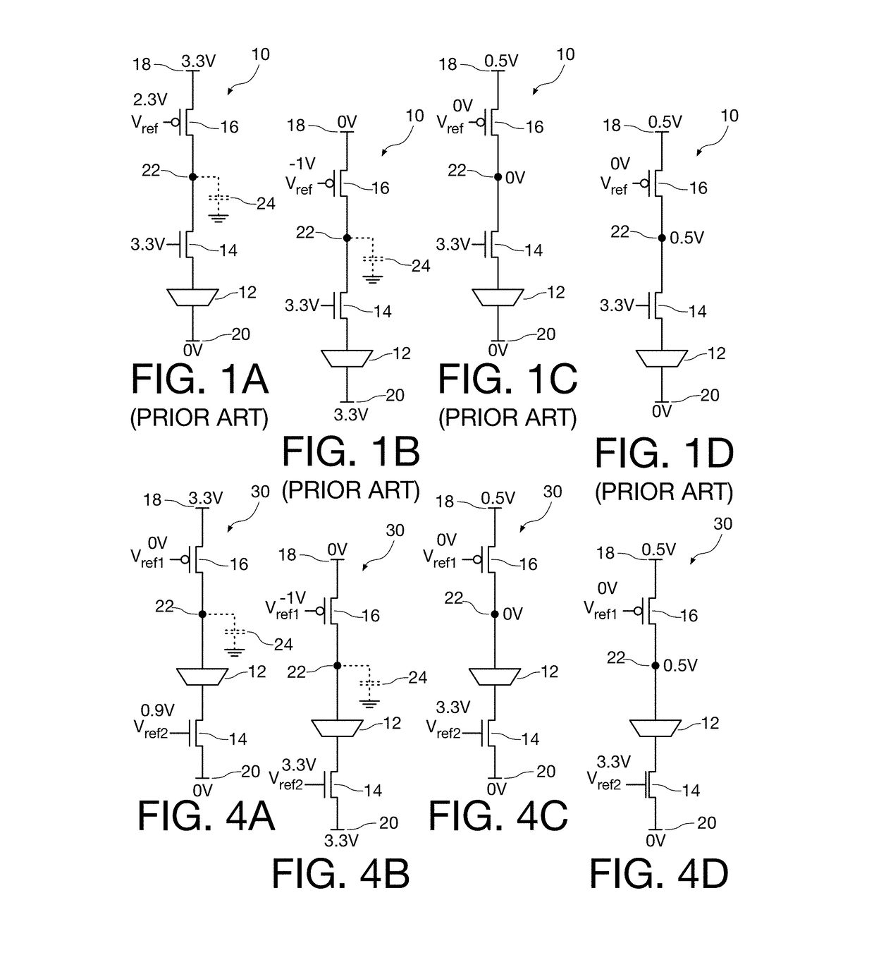
[0040]Referring now to FIGS. 4A through 4D, a 1T1R ReRAM memory cell 30 is depicted with various potentials applied to program, erase, and read the memory cell. Like ReRAM memory cell 10 of FIGS. 1A through 1D, ReRAM memory cell 30 includes ReRAM device 12, n-channel access transistor 14 and p-channel sense transistor 16 connected between bitlines 18 and 20. P-channel sense transistor 16 is connected between ReRAM device 12 and bitline 18, however n-channel access transistor 14 is advantageously connected between ReRAM device 12 and bitline 20. As is well known in the art bitlines 18 and 20 and the gates of transistors 14 and 16 may be selectively coupled to appropriate voltage potentials for programming, erasing, and reading the memo...


PUM


Abstract

A method for programming a ReRAM cell including a ReRAM device connected in series with an access transistor includes biasing the ReRAM cell with a programming potential that configures the access transistor in a common-source configuration and applying at least one programming voltage pulse to a gate of the access transistor, the programming voltage pulse having a magnitude selected to limit programming current to a preselected value.

Description

BACKGROUND[0001]The present invention relates to resistive random access memory (ReRAM) devices. More particularly, the present invention relates to circuitry and methods for programming ReRAM devices.[0002]ReRAM cells program by diffusion of metal ions through an electrolyte layer that is otherwise a barrier to electron flow. During programming an electric field (e-field) is presented across the device by placing appropriate potentials on the bit lines and word lines to which the cell is connected. The e-field increases until it causes breakdown of the electrolyte as the metal filament diffuses through the electrolyte from the ion source side of the device and reaches the opposite electrode. This often results in damage to the electrolyte, which makes the device difficult to erase and may even lead to device failure. A reverse e-field is applied to erase the device. The ion source of each of the ReRAM cells, throughout this document, is illustrated by the wider end.[0003]Attempts t...

Claims


Application Information

Patent Timeline
Patent Type & Authority Applications(United States)
IPC IPC(8): G11C13/00G11C5/06H01L27/24
CPCG11C13/0069G11C13/0028G11C13/0011G11C13/003G11C5/063H01L27/2454G11C2013/0078G11C2013/0073G11C2013/0071G11C13/004G11C13/0064G11C13/0097G11C2013/0045G11C2013/0092G11C2213/82H10B63/30H10N70/245H10N70/8416H10B63/34
Inventor MCCOLLUM, JOHN L.
Owner MICROSEMI SOC
Why Eureka
Try Eureka