

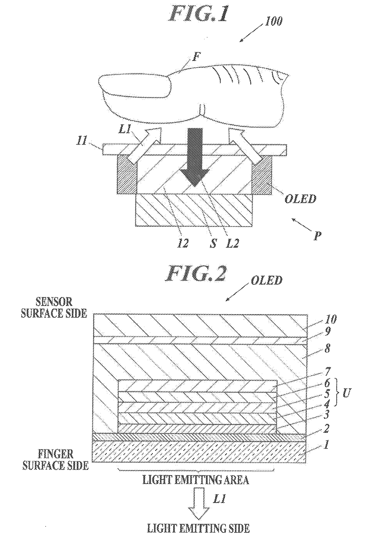
Optical fingerprint authentication device
a fingerprint authentication and optical technology, applied in the field of optical fingerprint authentication devices, can solve the problems of difficulty in processing led into a shape having a curved surface, the device is not easily miniaturized or suitable for mobile devices such as laptops, pda, cellular phones, etc., and achieve the effect of improving the recognition ra
- Summary
- Abstract
- Description
- Claims
- Application Information
AI Technical Summary
Benefits of technology
Problems solved by technology
Method used
Image

Examples
embodiment 1
thod 1 of Organic EL Panel
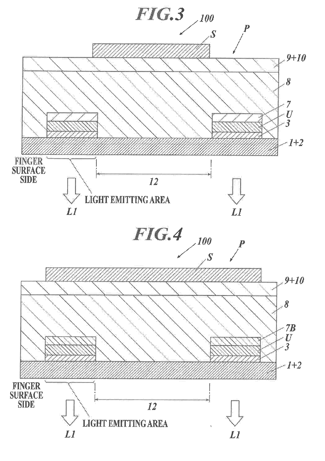
[0157]FIG. 3 is a schematic cross-sectional view showing an exemplary structure of the organic EL panel (P) according to the invention having an organic EL element (Embodiment 1).
[0158]The organic EL panel (P) illustrated in FIG. 3 has independent light emission areas shaped by arranging organic EL panels separate from each other on a transparent base material (1) having light transmittance in the organic EL element described in reference to FIG. 2 above. For more details, on the transparent base material (1) having the gas barrier layer (2) are arranged a plurality of organic EL elements (OLEDs) constituted by, for example, the anodes (3), the organic functional layer units (U), the cathodes (7), and so forth.
[0159]According to the structure illustrated in FIG. 3, the light emitting areas are regions in which all of the anode (3), the organic functional layer unit (U), and the cathode (7) exist. A region between the light emitting areas is the light-transm...
embodiment 2
thod 2 of Organic EL Panel
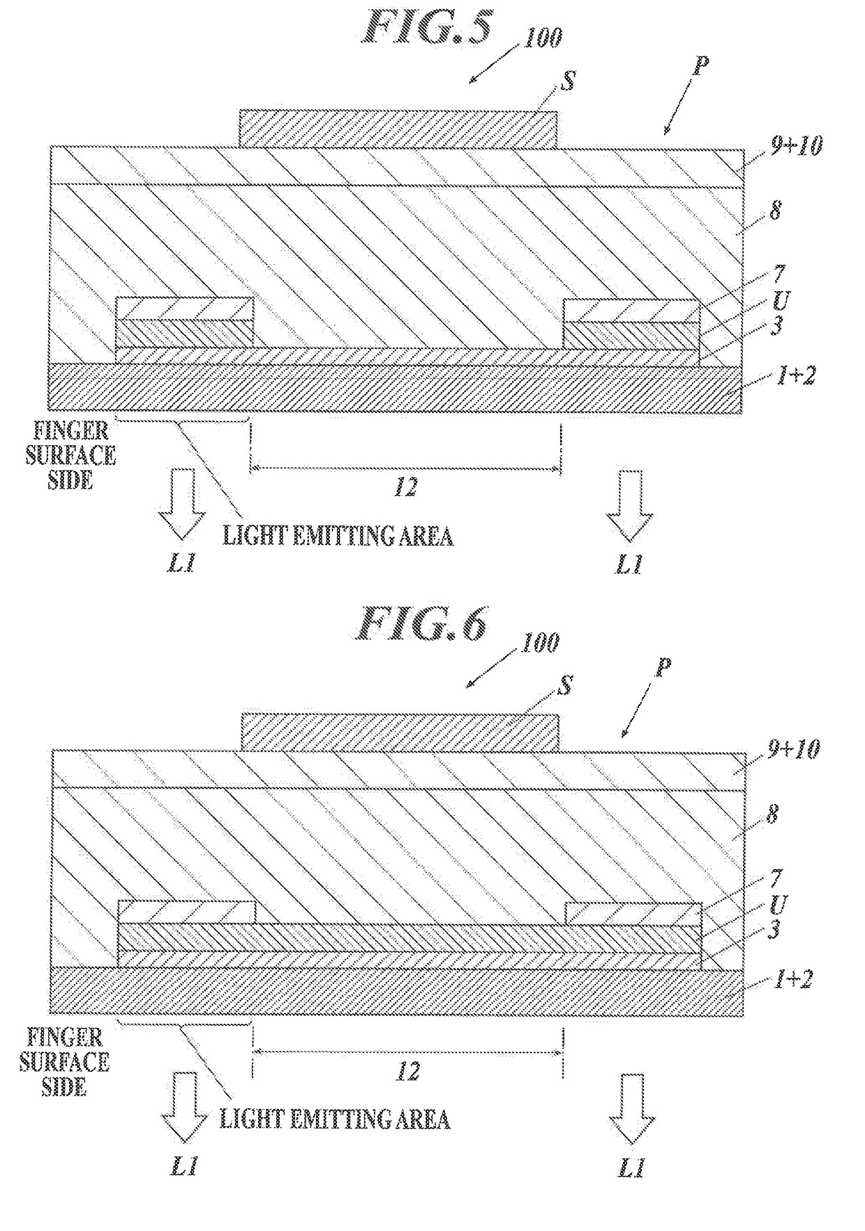
[0161]The organic EL panel (P) having a structure illustrated in FIG. 4 shows another exemplary structure in which the cathodes (7) are constituted by non-light transmitting electrodes, in particular, in the structure explained above in reference to FIG. 3. Such structure prevents irradiation of the image sensor side with irregular light which affects the measurement accuracy of the image sensor from the cathode (7) side of the organic EL element. Accordingly, the image sensor (S) can be arranged on the entire surface including the light emitting area.
embodiment 3
thod 3 of Organic EL Panel
[0162]The organic EL panel (P) having the structure illustrated in FIG. 5 shows a method of forming the organic EL element in which the light-transmitting anode (3) is formed at the entire surface of the light emitting area and the non-light emitting portion (12), so that only the organic functional layer units (U) and the cathodes (7) shape the light emitting area.
[0163]The light emitting area is required to have a structure in which all of the anode (3), the organic functional layer units (U), and the cathodes (7) are present in a single plane. As illustrated in FIG. 5, the region in which only the anode (3) is present functions as the non-light emitting portion (12).
PUM
 Abstract
Description
Claims
Application Information