
Light emitting diode (LED) mass-transfer apparatus and method of manufacture

a technology of light-emitting diodes and mass-transfer equipment, which is applied in electrical equipment, semiconductor devices, and testing/measurement of semiconductor/solid-state devices, etc., can solve the problems of inability to print kgd devices, inability to meet the requirements of micro-transfer-print systems (over 1500), and current approaches suffer from limitations in each of these criteria. , to achieve the effect of mass-production scale manufacturing, rapid and accurate placement of led device structures, and low cos

Active Publication Date: 2018-12-27
APPLE INC
View PDF6 Cites 18 Cited by
  • Summary
  • Abstract
  • Description
  • Claims
  • Application Information

AI Technical Summary

Benefits of technology

The patent describes a method for mass-producing LED structures using a laser beam to transfer LED devices from a source substrate to a target substrate. The method allows for the rapid and accurate placement of LED device structures with a high throughput and low error rate. The key benefit is the ability to produce LED devices at a high rate, making it compatible with high-volume manufacturing lines.

Problems solved by technology

Current approaches suffer from limitations in each of these criteria.
The throughput is claimed to exceed about 1 million LEDs per hour and that the method has limited to non-existent ability to print KGD devices.
These limitations are believed to be a fundamental result of the physical pick and place approach and difficult to further improve.
Assuming a 1 TV / minute rate of manufacture for a large-scale TV manufacturing line, an impractical number of micro-transfer-print systems (over 1500) are required.
Moreover, post-transfer printing repair will be a major reduction in effective throughput and require substantial rework.
The reliance on post-transfer repair is not only impractical but expensive and fraught with yield and quality issues.

Method used


Image

  • Light emitting diode (LED) mass-transfer apparatus and method of manufacture
  • Light emitting diode (LED) mass-transfer apparatus and method of manufacture
  • Light emitting diode (LED) mass-transfer apparatus and method of manufacture

Examples


example 1

esolution (3840H×2160V 16:9) BAR Mass-Transfer Performance Estimate

[0101]The following is the expected optimum throughput expected for the above laser conditions using a source substrate with 105 mm×105 mm LED device array of 15 μm pitch. The throughput will be somewhat less since it will not account for source substrate exchange time and site to site move time:[0102]a. Sub-pixel pitch: 125 μm (H)×375 μm (V)[0103]b. Number of sites: 11,650 cm2 display / 110.25 cm2=106 sites / display[0104]c. Pixels per scan line (H): 105 mm / 125 μm=840 pixels per scan[0105]d. Number of scan lines per site: 105 mm / 375 μm=280 lines[0106]e. Site throughput: 280 scan lines×19 msec=5.32 seconds / site[0107]f. Total pixels per site: 280 scans / site×840 pixels per scan=235,200 pixels / site[0108]g. Total time per display: 5.32 seconds / site×106 sites / display=564 seconds / display[0109]h. Pixel throughput=160M pixels / hour

[0110]The tremendous throughput improvement potential of this method can be appreciated by comparing...

example 2

Cellphone Display (1920H×1080V 16:9) BAR Mass-Transfer Performance Estimate

[0111]The following is the expected optimum throughput expected for the above laser conditions using a source substrate with 105 mm×105 mm LED device array of 15 μm pitch. The throughput will be somewhat less since it will not account for source substrate exchange time and site to site move time:[0112]a. Scan time: 68.5 mm / 7500 mm / sec=9.13 msec (scan in display vertical direction)[0113]b. Sub-pixel pitch: 21.1 μm (H)×63.4 μm (V)[0114]c. Number of sites: 1.16 sites / display[0115]d. Pixels per scan line (V): 68.5 mm / 63.4 μm=1080 pixels per scan[0116]e. Number of scan lines per site: 105 mm / 21.1 μm=4975 lines[0117]f. Site throughput: 4975 scan lines×13.13 msec=65.3 seconds / site[0118]g. Total pixels per site: 4975 scans / site×1080 pixels per scan=5.37M pixels / site[0119]h. Total time per display: 65.3 seconds / site×1.16 sites / display=75.7 seconds / display[0120]i. Pixel throughput=296M pixels / hour

[0121]The above exampl...


PUM


Abstract

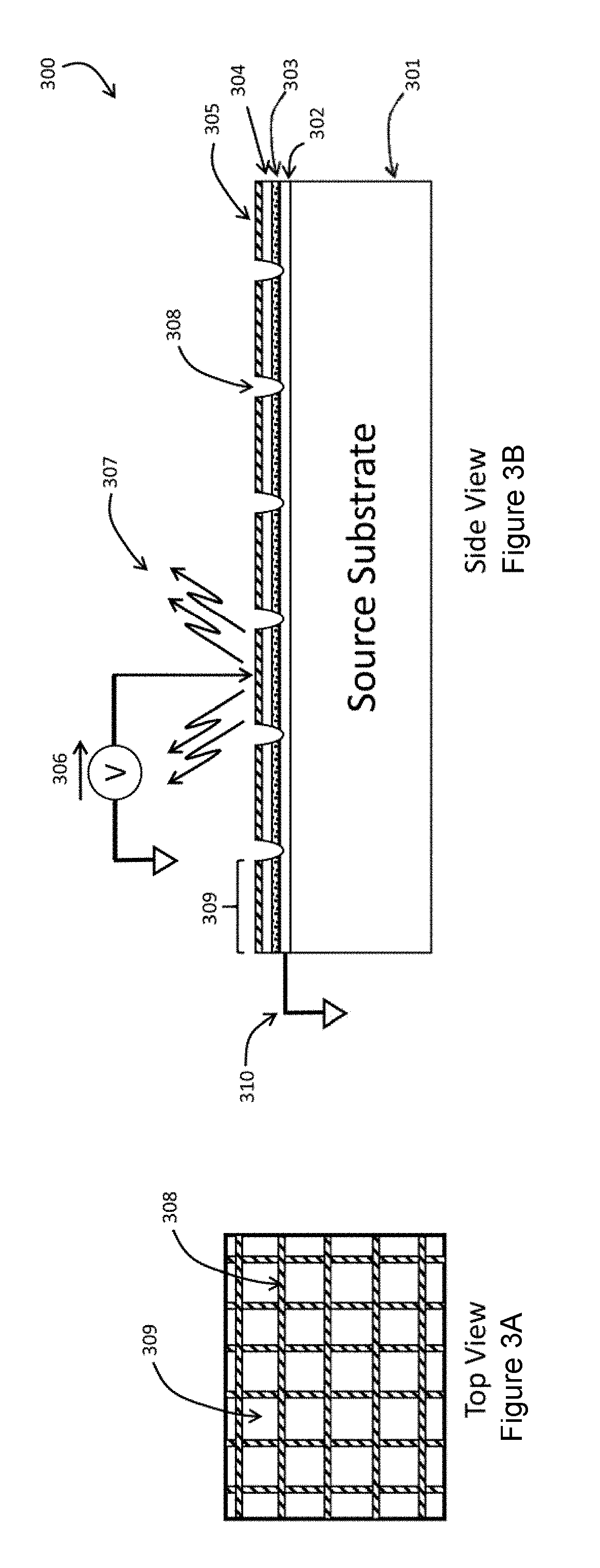
Embodiments relate to mass-transfer methods useful for fabricating products containing Light Emitting Diode (LED) structures. LED arrays are transferred from a source substrate to a target substrate by beam-assisted release (BAR) of a plurality of LED devices in a high-speed flexible manner. The BAR mass-transfer approach is also able to utilize a Known Good Die (KGD) data file of the source substrate to transfer only functionally good die and avoid rework and yield losses.

Description

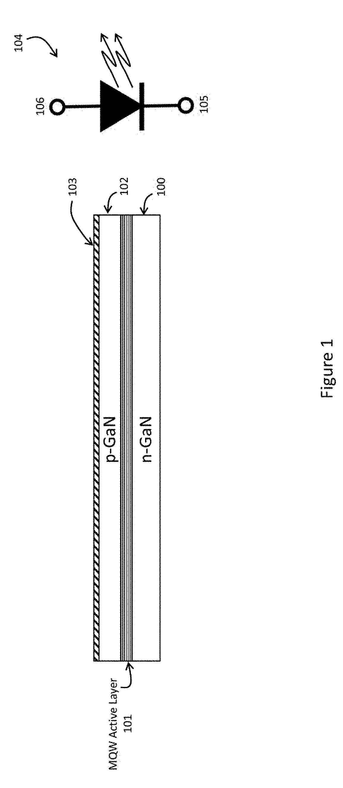
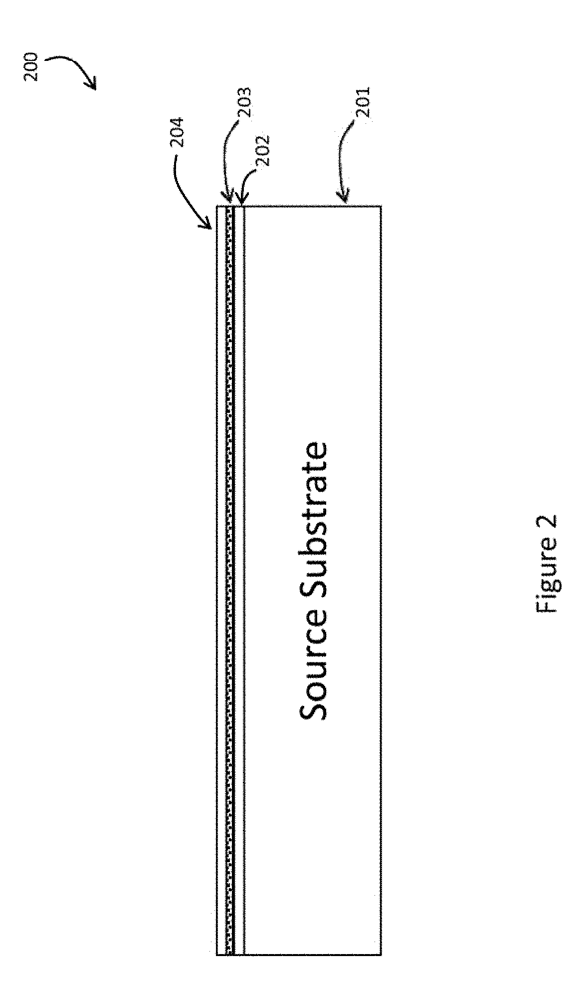
[0001]This application is a nonprovisional of U.S. Patent Application No. 62 / 525,105 filed Jun. 26, 2017, the contents of which are incorporated by reference herein.FIELD OF INVENTION[0002]The present invention relates to light emitting diode (LED) devices. More particularly, embodiments of the invention relate to techniques, including methods and apparatus to efficiently transfer a plurality of Light Emitting Diode (LED) devices from a source surface to a target surface during the manufacturing process. In an example, the method is useful in general LED device transfer and placement and is particularly useful for mass-transfer of micro-LED (uLED) devices that can be as small as a few microns on a side. Micro-LEDs are grown on a support substrate utilizing techniques such as Metallo-Organic Chemical Vapor Deposition (MOCVD) among others. Before the individual devices are used in their final lighting or display application, it is desirable to test the LED devices to establish Known G...

Claims


Application Information

Patent Timeline
IPC IPC(8): H01L25/075H01L33/00H01L25/16H01L21/66
CPCH01L25/0753H01L33/0079H01L25/167H01L22/20H01L33/32H01L33/06H01L21/78H01L33/00H01L33/0095H01L21/7806H01L21/67144H01L21/67132H01L21/67288H01L21/67271H01L33/0093H01L27/156H01L33/02H01L33/0075
Inventor HENLEY, FRANCOIS J.
Owner APPLE INC
Learn More