Semiconductor package and semiconductor package manufacturing method

a semiconductor and semiconductor technology, applied in the field of semiconductor package, can solve the problems of increased manufacturing cost, contact failure between the shield layer and the ground line, etc., and achieve the effect of increasing manufacturing cos

Inactive Publication Date: 2019-01-03
DISCO CORP
View PDF2 Cites 0 Cited by
  • Summary
  • Abstract
  • Description
  • Claims
  • Application Information

AI Technical Summary

Benefits of technology

[0009]According to the present invention, the contact metal is formed so as to cover the ground line exposed to the side surface of the redistribution layer. Accordingly, the ground line can be reliably connected through the contact metal to the shield layer formed on the side surface of the semiconductor package.
[0010]The above and other objects, fe...

Problems solved by technology

However, since the redistribution layer is thin, there is a possibility that a contact failure may occur b...

Method used


Image

  • Semiconductor package and semiconductor package manufacturing method
  • Semiconductor package and semiconductor package manufacturing method
  • Semiconductor package and semiconductor package manufacturing method

Examples


Embodiment Construction

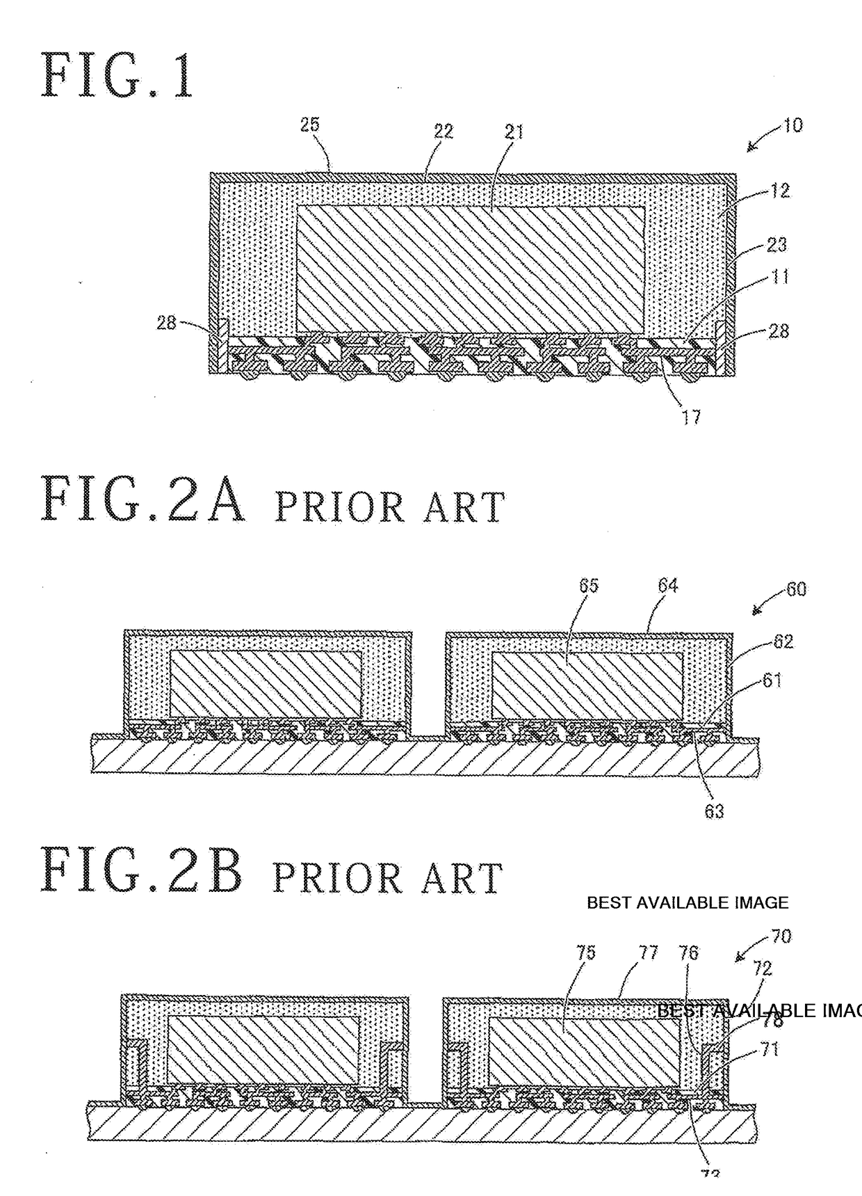
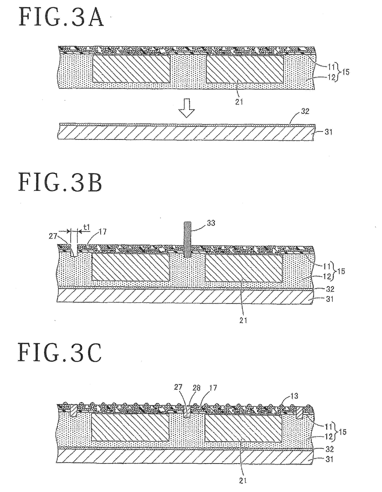
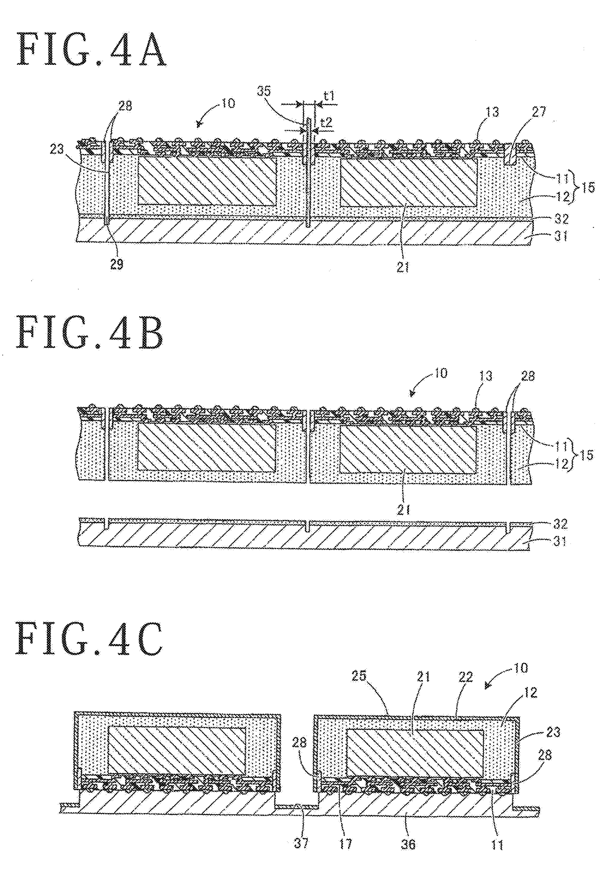
[0017]A semiconductor package manufacturing method according to a preferred embodiment of the present invention will now be described with reference to the attached drawings. FIG. 1 is a schematic sectional view of a semiconductor package to be manufactured according to this preferred embodiment. FIGS. 2A and 2B are sectional views of conventional semiconductor packages as different comparisons. The following preferred embodiment is merely illustrative, and another step may be added between steps. Further, the order of steps may be suitably changed.

[0018]Referring to FIG. 1, there is depicted a semiconductor package 10 according to this preferred embodiment. The semiconductor package 10 is a so-called fan-out wafer level package or the like such that a redistribution area is larger than a chip size. The semiconductor package 10 includes a redistribution layer 11 and a semiconductor chip 21 connected to the redistribution layer 11. The semiconductor chip 21 is sealed with a resin lay...


PUM


Abstract

Disclosed herein is a semiconductor package including a redistribution layer and a semiconductor chip connected to the redistribution layer, the semiconductor chip being sealed with a resin layer, the redistribution layer including a ground line exposed to the side surface of the redistribution layer. The semiconductor package includes a contact metal formed on the side surface of the redistribution layer so as to cover the ground line and a shield layer formed on the upper surface and the side surface of the semiconductor package so as to cover the contact metal. The shield layer is connected through the contact metal to the ground line exposed to the side surface of the redistribution layer.

Description

BACKGROUND OF THE INVENTIONField of the Invention[0001]The present invention relates to a semiconductor package having a shielding function and a manufacturing method for such a semiconductor package.Description of the Related Art[0002]In general, a semiconductor package for use in portable communications equipment such as mobile phones is required to suppress the leakage of electromagnetic noise from the semiconductor package, so as to prevent any adverse effect on communications characteristics. As an example of the semiconductor package, there is a configuration such that a semiconductor chip mounted on a distribution layer (wiring layer) is sealed with resin (sealing agent) to form a resin layer, and a shield layer is formed on the outer surface of the resin layer (see Japanese Patent Laid-Open No. 2012-039104, for example). There is a case that the shield layer is formed from a sheet metal. However, since the sheet metal has a large thickness, it causes an interference with a r...

Claims


Application Information

Patent Timeline
IPC IPC(8): H01L23/552H01L23/528
CPCH01L23/552H01L23/5286H01L21/56H01L23/31H01L2924/181H01L2224/16225H01L2224/97H01L21/6835H01L2221/68331H01L23/3121H01L2924/00012H01L24/05H01L24/03H01L24/27H01L24/29
Inventor JANG, BYEONGDECKKIM, YOUNGSUK
Owner DISCO CORP
Why Eureka
Try Eureka