Highly efficient double-sampling architectures

a double-sampling, high-efficiency technology, applied in the direction of measurement devices, instruments, measurement devices, etc., can solve the problems of inacceptability, area and power costs, and inability to meet the requirements of measurement, so as to achieve cost reduction and design

Inactive Publication Date: 2019-01-10
NICOLAIDIS MICHEL
View PDF18 Cites 3 Cited by
  • Summary
  • Abstract
  • Description
  • Claims
  • Application Information

AI Technical Summary

Benefits of technology

This patent presents innovations to improve the efficiency of double-sampling architectures in terms of area, power cost, and error detection efficiency. Specifically, it presents a double-sampling architecture with timing constraints and enforcement procedures to reduce area and power cost by eliminating redundant sampling elements. It also introduces a unbalanced comparator implementation approach to reduce the number of buffers required and increase comparator speed. Additionally, it introduces architectures accelerating the speed of comparators by introducing hazards-blocking cells. Finally, it presents a low-cost approach for metastability mitigation of error detecting designs to reduce the number of latches checked by the double-sampling scheme.

Problems solved by technology

The resulting high defect levels affect adversely fabrication yield and reliability.
However, area and power penalties exceed 100% and are inacceptable for a large majority of applications.
The other source of area and power cost is the enforcement of the short path constraint.
Thus, this element will capture data different than those captured by the regular flip-flop and will produce false error detection.
Enforcing this constraint will require adding buffers in some short paths to increase their delays at a value larger than δ+th, inducing area and power cost.
The use of redundant sampling elements is one of the two major sources of area cost and more importantly of power cost, as sequential elements are the most power consuming elements of a design.
We note that from the above arguments the scheme of FIG. 2 enables detection of timing faults of duration up to δ. However, the analysis in [7] is incomplete, and does not guarantee the system to operate flawlessly.
Also, as illustrated next the architecture of FIG. 2 is non-conventional as it violates a fundamental constraint of synchronous designs.
Thus, the timing constraints required for the flawless operation of this architecture cannot be enforced by existing design automation tools.
However, employing two clock trees will induce significant area and power cost.
However, if the delay Dcomp+δ is large, it can be subject to non-negligible variations that may affect flawless operation.
As the Comparator 30 may check a large number of regular flip-flops, adding such delays will induce significant area and power penalties.
However, for the non-conventional synchronous design of this Fig., the author wrongly sets the short path constraint by means of maximum circuit delays.
As we will show later, the short path constraint imposed by [18] is too strong increasing unnecessary area and power costs.
We will also show that, the implementation proposed in [18] does not guarantee flawless operation, as some other constraints concerning long paths are also necessary for guarantying it.
Hence, the existing state of the art specifies the conditions required for the flawless operation of the architecture of FIG. 2 incorrectly and incompletely and can not be used to implement designs operating flawlessly.
The major difficulty for specifying correctly these conditions is that this design is non-conventional, because it does not satisfy a fundamental constraint in synchronous designs: the propagation delays between to consecutive pipeline stages should be lesser than the clock period.

Method used


Image

  • Highly efficient double-sampling architectures
  • Highly efficient double-sampling architectures
  • Highly efficient double-sampling architectures

Examples


Embodiment Construction

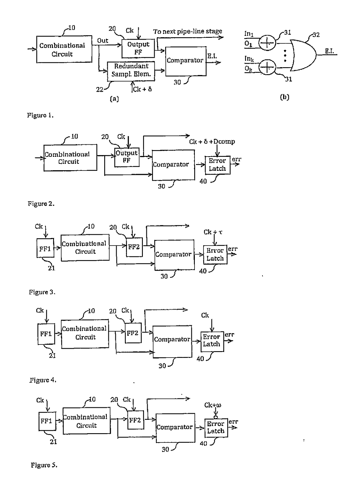
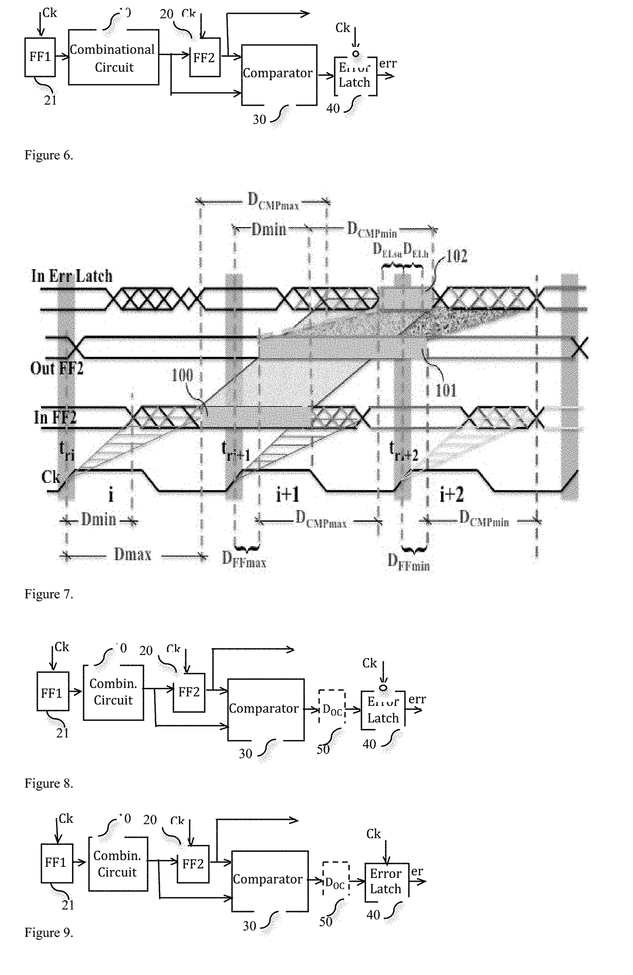
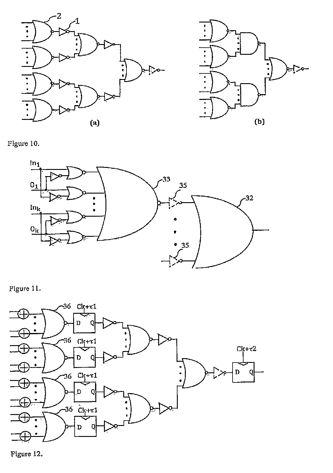
[0049]The goal of the present invention is to propose implementations minimizing the cost of the double-sampling scheme of FIG. 2; derive the conditions guarantying its flawless operation; provide a methodology allowing enforcing these conditions by means of manual implementation or for developing dedicated automation tools; implement these constraints conjointly for the combinational circuit and the comparator in a manner that reduces cost and increases speed; propose fast comparator designs by exploiting the specificities of the error detection circuitry; enhance double-sampling to mitigate single-event upsets without increasing cost. In the following, we first present a systematic theory, which is a fundamental support for describing these enhancements. Certain parts of this analysis and some of the related improvements are based on our previous publication [22].

Elimination of Redundant Sampling Elements and Related Timing Constraints

[0050]In the double sampling scheme of FIG. 3,...


PUM

PropertyMeasurementUnit
sensitivityaaaaaaaaaa

Abstract

Aggressive technology scaling impacts parametric yield, life span, and reliability of circuits fabricated in advanced nanometric nodes. These issues may become showstoppers when scaling deeper to the sub-10nm domain. To mitigate them various approaches have been proposed including increasing guard-bands, fault-tolerant design, and canary circuits. Each of them is subject to several of the following drawbacks; large area, power, or performance penalty; false positives; false negatives; and in sufficient coverage of the failures encountered in the deep nanometric domain. The invention presents a highly efficient double-sampling architecture, which allow mitigating all these failures at low area and performance penalties, and also enable significant power reduction.

Description

[0001]This application is a continuation of U.S. patent application Ser. No. 15 / 858,205 filed Dec. 29, 2017, which is a continuation of U.S. patent application Ser. No. 15 / 393,035 filed Dec. 28, 2016, which in turn is a non-provisional application of U.S. Provisional Patent Application No. 62 / 271,778 filed Dec. 28, 2015. The entire disclosures of these applications are incorporated herein by reference.BACKGROUND OF THE INVENTION[0002]The present invention relates to double-sampling architectures, which reduces the cost for detecting errors produced by temporary faults, such as delay faults, clock skews, single-event transients (SETs), and single-event upsets (SEUs), by avoiding circuit replication and using instead the comparison of the values present on the outputs of a circuit at two different instants.STATE OF THE ART[0003]Aggressive technology scaling has dramatic impact on: process, voltage, and temperature (PVT) variations; circuit aging and wearout induced by failure mechanis...

Claims


Application Information

Patent Timeline
Patent Type & Authority Applications(United States)
IPC IPC(8): G01R31/317H03K19/003
CPCH03K19/003G01R31/31725G01R31/31727G01R31/31703G01R31/3172
Inventor NICOLAIDIS, MICHEL
Owner NICOLAIDIS MICHEL
Why Eureka
Try Eureka