Solid-state source of atomic specie for etching

a solid-state source and atomic specie technology, applied in the direction of electrical equipment, basic electric elements, electric discharge tubes, etc., can solve the problems of hydrogen damage to the electrical characteristics of the mram device, the processing of mram features with smart vertical sidewalls, and the difficulty of magnetic resistance random access memory devices

Inactive Publication Date: 2019-01-31
TOKYO ELECTRON LTD
View PDF1 Cites 0 Cited by
  • Summary
  • Abstract
  • Description
  • Claims
  • Application Information

AI Technical Summary

Benefits of technology

[0009]Note that this summary section does not specify every embodiment and / or incrementally novel aspect of the present disclosure or claimed invention. Instead, this summary only provides a preliminary discussion of different embodiments and corresponding points of novelty over conventional techniques. For additional details and / or possible perspectives of the invention and embodiments, the reader is directed to the Detailed Description section and corresponding figures of the present disclosure as further discussed below.

Problems solved by technology

The manufacture of magneto-resistive random access memory (MRAM) devices presents many challenges to device manufacturers and equipment suppliers, particularly with patterning the complex metal stacks.
One of the major hindrances in the processing of MRAM features with smart vertical sidewalls derives from the origin of the carbon source used for their passivation.
Carbon is usually delivered with hydrogen; however, hydrogen can damage the electrical characteristics of the MRAM device.
Furthermore, carbon, introduced as a compound into plasma, dissociates into constituents of the compound in a relatively uncontrollable manner.
As a result, the byproducts of uncontrollable dissociation can form polymer layers that inhibit robust patterning of metal stacks with proper profile control.

Method used


Image

  • Solid-state source of atomic specie for etching
  • Solid-state source of atomic specie for etching
  • Solid-state source of atomic specie for etching

Examples


Embodiment Construction

[0018]Techniques herein pertain to device fabrication using precision etch techniques. Several instances manifest in semiconductor manufacturing in both logic and memory device. As an example, it is important to transfer patterns into the metal stacks that form magneto-resistive random access memory (MRAM) with accurate control of the profile.

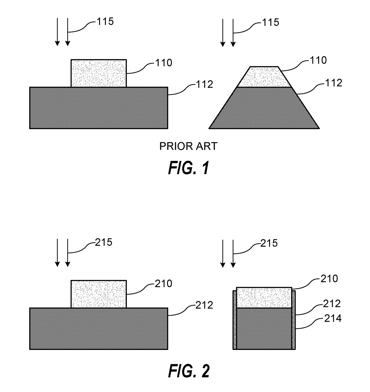
[0019]As noted above, one of the major hindrances in the processing of MRAM features with smart vertical sidewalls derives from the origin of the carbon source used for their passivation. For example, FIG. 1 illustrates a method of patterning an MRAM stack 112, wherein a patterned mask 110 overlies the MRAM stack 112, and the pattern is extended into MRAM stack 112 using a conventional ion milling process. However, as shown, the ion milling process has poor profile control, leading to a tapered stack.

[0020]As another example, FIG. 2 illustrates a method of patterning an MRAM stack 212, wherein a patterned mask 210 overlies the MRAM stack 212, a...


PUM


Abstract

An etching system, a solid state source for supplying an atomic specie, and a method of operating are described. The system includes: a processing chamber for treating a substrate in a gas-phase chemical environment; a substrate holder for supporting the substrate in the processing chamber; and a solid state source of an atomic specie coupled to the processing chamber, and configured to supply the atomic specie to the processing chamber when treating the substrate. The processing chamber can facilitate a gas-phase, plasma-containing or non-plasma-containing environment.

Description

CROSS-REFERENCE SECTION[0001]This application claims priority to Provisional Patent Application No. 62 / 536,723, entitled, SOLID-STATE SOURCE OF ATOMIC SPECIE FOR ETCHING, filed Jul. 25, 2017; the disclosure of which is expressly incorporated herein, in its entirety, by reference.FIELD OF INVENTION[0002]The invention relates to an apparatus and method for etching, and more particularly, a precision etch apparatus and technique for etching a thin film for electronic device applications.BACKGROUND OF THE INVENTION[0003]The manufacture of magneto-resistive random access memory (MRAM) devices presents many challenges to device manufacturers and equipment suppliers, particularly with patterning the complex metal stacks. One of the major hindrances in the processing of MRAM features with smart vertical sidewalls derives from the origin of the carbon source used for their passivation. Carbon is usually delivered with hydrogen; however, hydrogen can damage the electrical characteristics of t...

Claims


Application Information

Patent Timeline
Patent Type & Authority Applications(United States)
IPC IPC(8): H01J37/32
CPCH01J37/3244H01J2237/3341H01J2237/006H01J2237/3132H01J2237/334H10N50/01H10N50/00
Inventor VENTZEK, PETERRANJAN, ALOK
Owner TOKYO ELECTRON LTD
Why Eureka
Try Eureka