Method of plasma etching of silicon-containing organic film using sulfur-based chemistry

Active Publication Date: 2018-12-13
TOKYO ELECTRON LTD
View PDF2 Cites 0 Cited by
  • Summary
  • Abstract
  • Description
  • Claims
  • Application Information

AI Technical Summary

Benefits of technology

[0008]Note that this summary section does not specify every embodiment and/or incrementally novel aspect of the present disclosure or claimed invention. Instead, this summary only provides a preliminary discussion of different embodiments and corresponding points

Problems solved by technology

Scaling efforts have greatly increased the number of transistors per unit area in 2D circuits, yet scaling efforts are running into greater challenges as scaling enters single digit nanometer semiconductor device fabrication nodes.
Trade-offs between selectivity, profile, ARDE (aspect ratio dependen

Method used


Image

  • Method of plasma etching of silicon-containing organic film using sulfur-based chemistry
  • Method of plasma etching of silicon-containing organic film using sulfur-based chemistry

Examples


Embodiment Construction

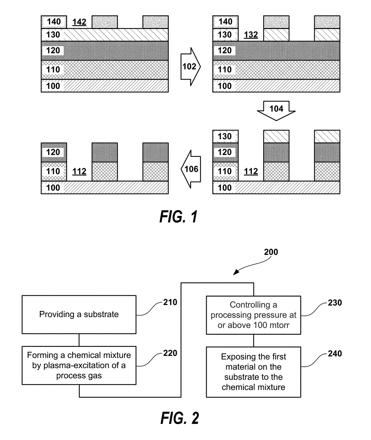
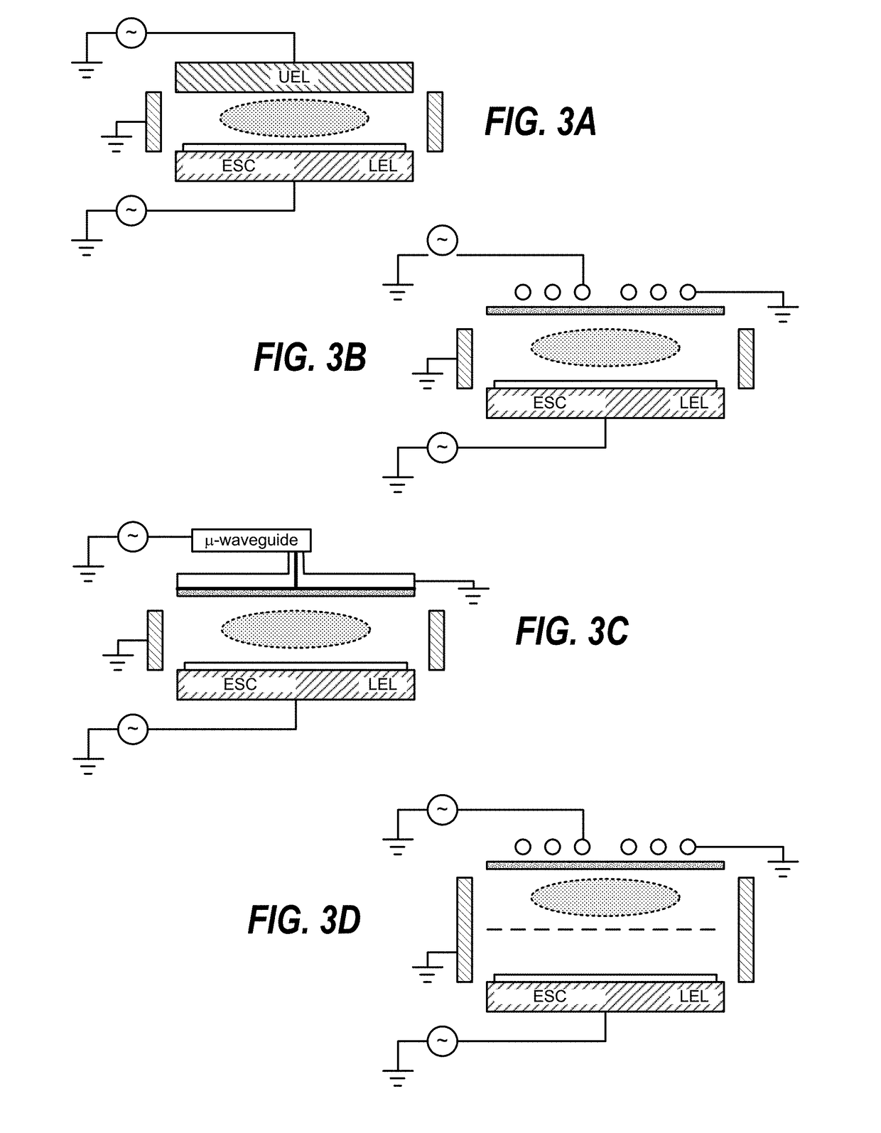
[0013]Techniques herein pertain to device fabrication using precision etch techniques. Several instances manifest in semiconductor manufacturing in both front end of line (FEOL, e.g., transistor fabrication) through to the back end of line (BEOL, e.g., interconnect fabrication), where mask layers, oxide and nitride films (typically silicon-containing, in nature), silicon and metal layers, etc. need to be etched with a high degree of precision.

[0014]Numerous fabrication sequences in semiconductor manufacturing demand precision etch techniques for both 2D (two-dimensional) and 3D (three-dimensional) device structures. Still, tri-layer etch masks (e.g., including photoresist, anti-reflective coatings (ARC), and organic carbon films) serve as the workhorse of patterning masks into the underlying layer. Current challenges involve obtaining pattern transfer with no loading artifacts, vertical sidewall profile and square bottom with immense selectivity to the ARC layer. Continuous plasma e...


PUM


Abstract

A method of etching is described. The method providing a substrate having a first material composed of silicon-containing organic material and a second material that is different from the first material, forming a chemical mixture by plasma-excitation of a process gas containing SF6 and an optional inert gas, controlling a processing pressure at or above 100 mtorr, and exposing the first material on the substrate to the chemical mixture to selectively etch the first material relative to the second material.

Description

RELATED APPLICATIONS[0001]This application claims priority to the following pending provisional application: U.S. Provisional Patent Application Ser. No. 62 / 516,941, filed Jun. 8, 2017, and entitled “METHOD OF PLASMA ETCHING OF SILICON-CONTAINING ORGANIC FILM USING SULFUR-BASED CHEMISTRY” which is hereby incorporated by reference in its entirety.FIELD OF INVENTION[0002]The invention relates to a method for etching, and more particularly, a precision etch technique for etching a thin film for electronic device applications.BACKGROUND OF THE INVENTION[0003]The present invention relates to a method of manufacturing a semiconductor device such as an integrated circuit and transistors and transistor components for an integrated circuit. In the manufacture of a semiconductor device (especially on the microscopic scale), various fabrication processes are executed such as film-forming depositions, etch mask creation, patterning, material etching and removal, and doping treatments, are perfo...

Claims


Application Information

Patent Timeline
IPC IPC(8): H01L21/311H01L21/3065H01L21/3213
CPCH01L21/31138H01L21/3065H01L21/32137H01L21/31144H01L21/0276H01L21/31116H01L21/32136H01L21/0274H01L21/0332H01L21/0337
Inventor KARAKAS, ERDINCWANG, LINOLAN, ANDREWTALONE, CHRISTOPHERSRIDHAR, SHYAMRANJAN, ALOKOHTAKE, HIROTO
Owner TOKYO ELECTRON LTD
Why Eureka
Try Eureka