Surface modification process

a surface modification and surface technology, applied in the field of surface modification methods and systems, can solve the problems of increasing the difficulty of scaling efforts, arde), and the difficulty of managing uniformity in plasma etching processes, and the current approach to patterning and pattern transfer by balancing these trade-offs is not sustainabl

Active Publication Date: 2020-03-05
TOKYO ELECTRON LTD
View PDF3 Cites 0 Cited by
  • Summary
  • Abstract
  • Description
  • Claims
  • Application Information

AI Technical Summary

Benefits of technology

[0009]Note that this summary section does not specify every embodiment and / or incrementally novel aspect of the present disclosure or claimed invention. Instead, this summary only provides a preliminary discussion of different embodiments and corresponding points of novelty over conventional techniques. For additional details and / or possible perspectives of the invention and embodiments, the reader is directed to the Detailed Description section and corresponding figures of the present disclosure as further discussed below.

Problems solved by technology

Scaling efforts have greatly increased the number of transistors per unit area in 2D circuits, yet scaling efforts are running into greater challenges as scaling enters single digit nanometer semiconductor device fabrication nodes.
Trade-offs between selectivity, profile, aspect ratio dependent etching (ARDE), and uniformity in plasma etch processes become difficult to manage.
Current approaches to patterning and pattern transfer by balancing these trade-offs is not sustainable.
The root cause for these trade-offs is the inability to control ion energy, ion flux, and radical flux independently.

Method used


Image

  • Surface modification process
  • Surface modification process
  • Surface modification process

Examples


Embodiment Construction

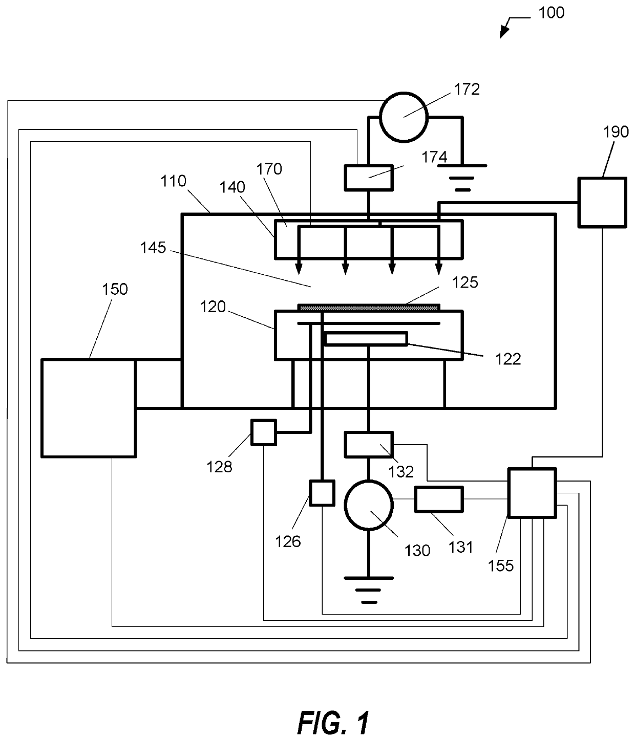
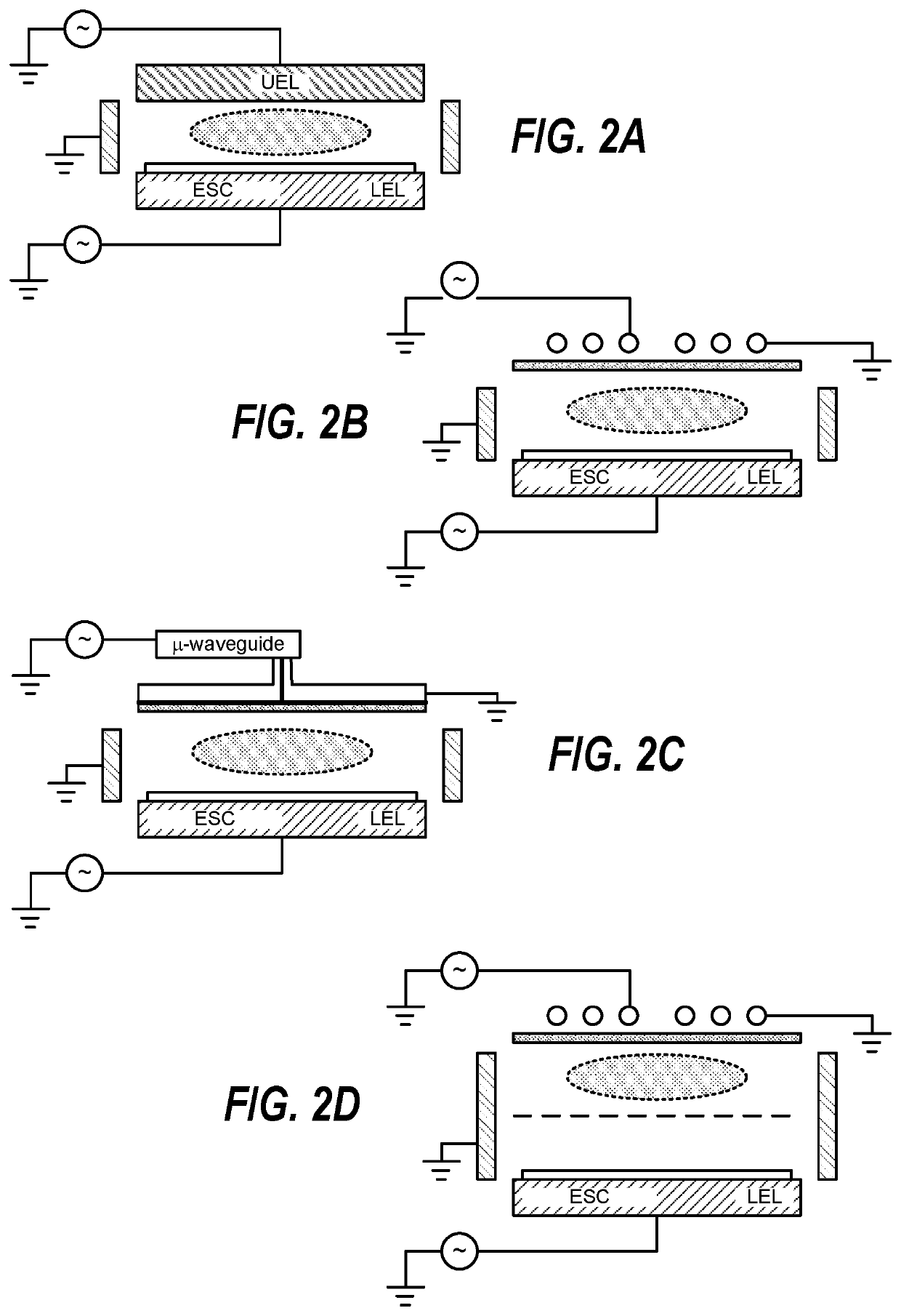
[0030]Techniques herein pertain to device fabrication using precision etch techniques. Several instances manifest in semiconductor manufacturing in both front end of line (FEOL, e.g., transistor fabrication) through to the back end of line (BEOL, e.g., interconnect fabrication), where oxide and nitride films (typically silicon-containing, in nature) need to be etched with a high degree of precision.

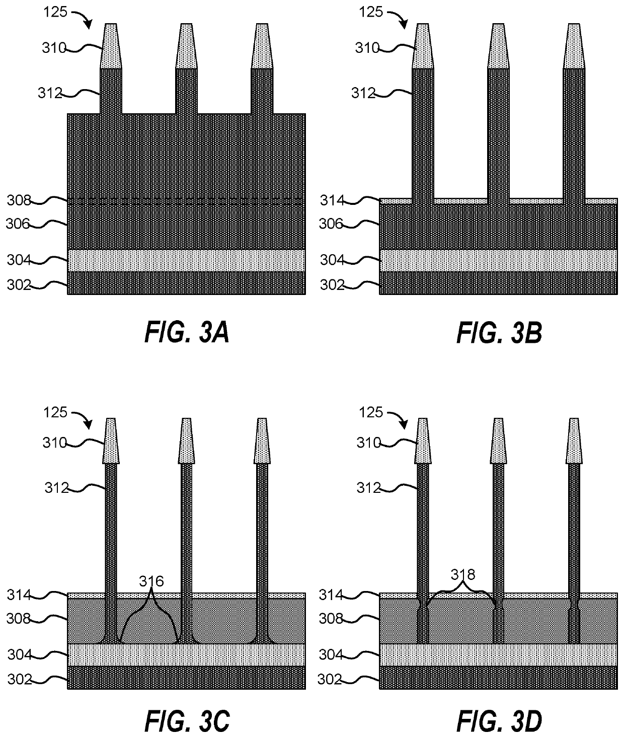
[0031]Numerous fabrication sequences in semiconductor manufacturing demand precision etch techniques. Examples, which will be discussed later, include: (1) gate spacer etch for both 2D (two-dimensional) and 3D (three-dimensional) device structures, (2) spacer etch for sidewall image transfer (SIT) for multi-patterning, (3) mandrel removal from a post-spacer etch SIT structure, and (4) liner etch from a raised structure.

[0032]During formation of various features on and / or in a semiconductor substrate, various etch steps are required. Various etch techniques may be used, including wet etch ...


PUM

PropertyMeasurementUnit
pressureaaaaaaaaaa
pressureaaaaaaaaaa
pressureaaaaaaaaaa

Abstract

Methods and systems for surface modification are described. In an embodiment, a method of etching includes providing a substrate having a device structure, portions of which are identified for modification. Such a method may also include passivating target surfaces of the device structure by exposing the device structure to a gas-phase composition at a processing pressure equal to or greater than 100 mTorr to form a protection layer on the target surfaces. Other embodiments of a method may include providing a substrate having a device structure, portions of which identified for removal. Such methods may further include passivating target surfaces of the device structure by exposing the device structure to a gas-phase composition, wherein the ratio of the radical content to the ion content exceeds 10-to-1.

Description

CROSS-REFERENCE TO RELATED APPLICATIONS[0001]This application claims priority to U.S. Provisional Application No. 62 / 727,167 filed on Sep. 5, 2018 which is hereby incorporated by reference in its entirety.FIELD OF INVENTION[0002]The invention relates to a method for etching, and more particularly, methods and systems for surface modification to reduce side wall etch.BACKGROUND OF THE INVENTION[0003]The present invention relates to a method of manufacturing a semiconductor device such as an integrated circuit. An integrated circuit may include transistors and transistor components. In the manufacture of a semiconductor device, various fabrication processes are executed such as film-forming depositions, etch mask creation, patterning, material etching and removal, and doping treatments. Such processes are performed, sometimes repeatedly, to form desired semiconductor device elements on a substrate. Historically, with microfabrication, transistors have been created in one plane, with w...

Claims


Application Information

Patent Timeline
Patent Type & Authority Applications(United States)
IPC IPC(8): H01L29/40H01L29/66H01L21/033H01L21/3213
CPCH01L21/0337H01L29/401H01L29/66795H01L21/32139H01L29/66818H01L29/66439H01L29/775B82Y10/00H01L29/0673H01L29/42376H01L21/02274
Inventor THOMAS, CEDRICNOLAN, ANDREWRANJAN, ALOK
Owner TOKYO ELECTRON LTD
Why Eureka
Try Eureka