

Semiconductor device and method for producing semiconductor device
- Summary
- Abstract
- Description
- Claims
- Application Information
AI Technical Summary
Benefits of technology
Problems solved by technology
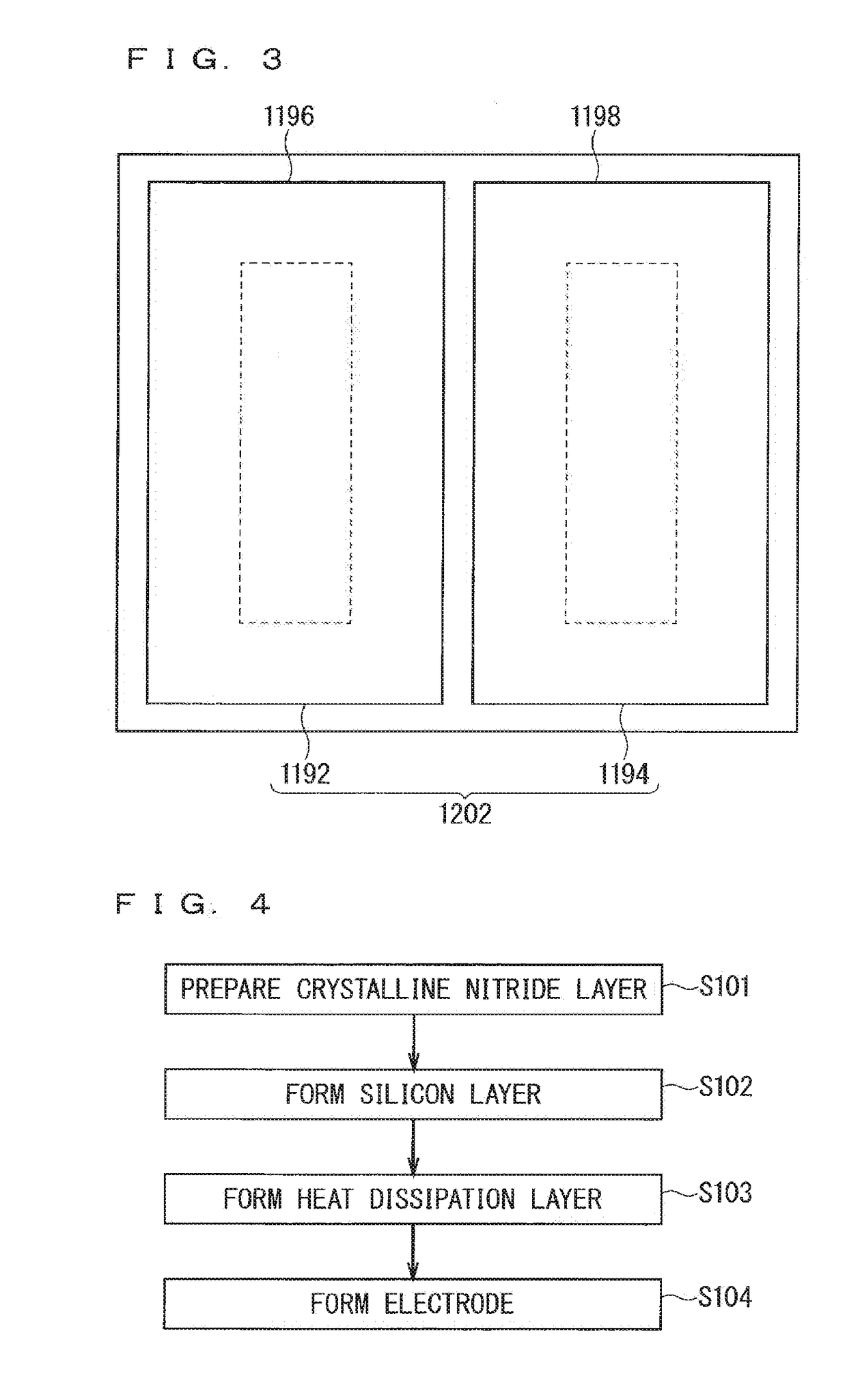
Method used
Image

Examples
Embodiment Construction
)
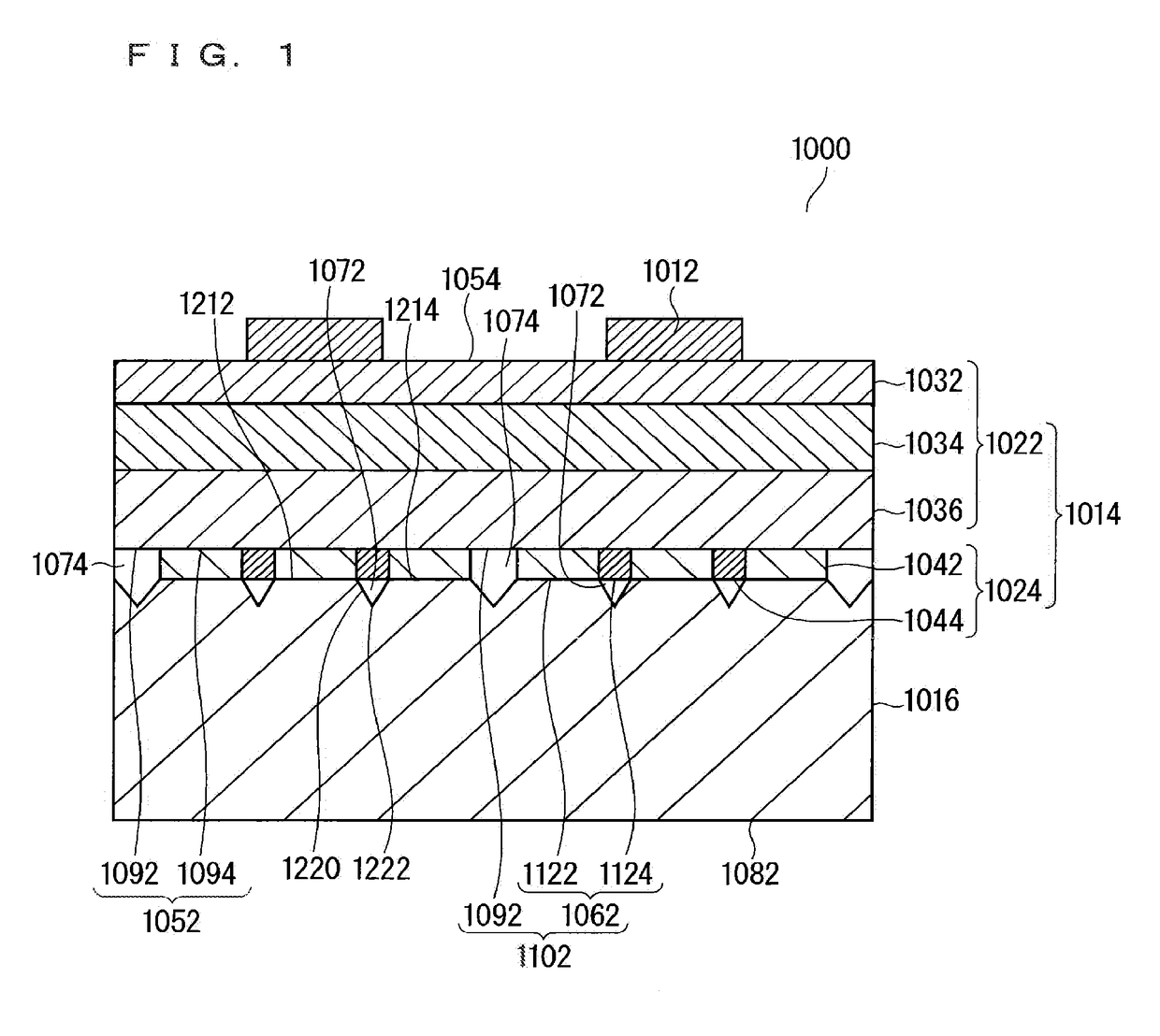
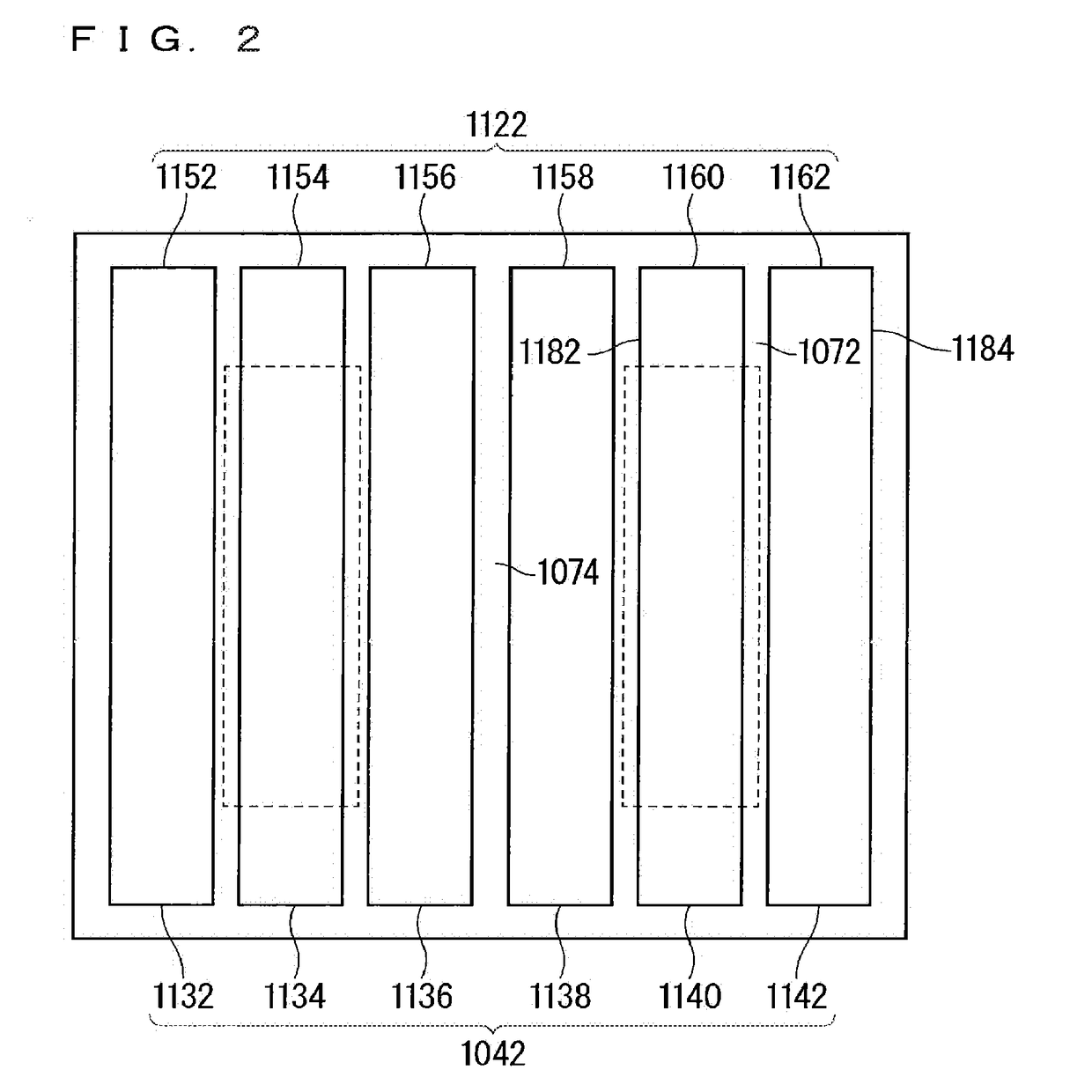
1. The First Preferred Embodiment
[0030]1.1 Causes of Cracking of Crystalline Nitride Layer in Semiconductor Device
[0031]Table 1 shows respective linear expansion coefficients and thermal conductivities of diamond, gallium nitride (GaN), aluminum nitride (AlN), and silicon (Si).
TABLE 1Linear Expansion CoefficientThermal ConductivityMaterials(×10−6 / K)(W / m · K)Diamond1.12000GaN5.6 (a axis)220AlN4.3170Si2.6150
[0032]As shown in Table 1, the thermal conductivity of diamond is remarkably larger than that of the group III nitride such as GaN, AlN, or the like. For this reason, in a case where diamond is used for heat dissipation in a semiconductor device which adopts the group III nitride, the heat dissipation performance of the semiconductor device is improved.
[0033]On the other hand, the linear expansion coefficient of diamond is remarkably smaller than that of the group III nitride such as GaN, AlN, or the like. For this reason, in a case where a diamond layer comes into contact with a ...
PUM
| Property | Measurement | Unit |
|---|---|---|
| Heat | aaaaa | aaaaa |
Abstract
Description
Claims
Application Information