
Eureka
For R&D, Eureka makes reading and utilizing patents & technical documents easy.
Eureka AIR
Designed for self-driven R&D workflows. Generate viable solutions, solve complex R&D challenges, empower your innovation with AI.

Eureka Materials
Designed for material experts only. Revolutionize your material R&D, from search, analyze, to developing new materials.

TechResearch
Generate reliable direction feasibility study reports for your R&D in just a few steps.

TechSeek
Discover and master advanced knowledge NOW. Basics, ideas, possibilities, all at once.

TechMind
As an expert in R&D Theories, TechMind can generates customized viable solutions instantly.

TechRisk
Analyze your overall solution with one click, know your potential R&D risks in advance.

TechMonitor
Get weekly tech updates, stay abreast of the latest tech innovations and key insights.
Method for producing crystalline film
- Summary
- Abstract
- Description
- Claims
- Application Information
AI Technical Summary
Benefits of technology
Problems solved by technology
Method used
Image

Examples
example 1
[0113]1. Forming a Buffer Layer
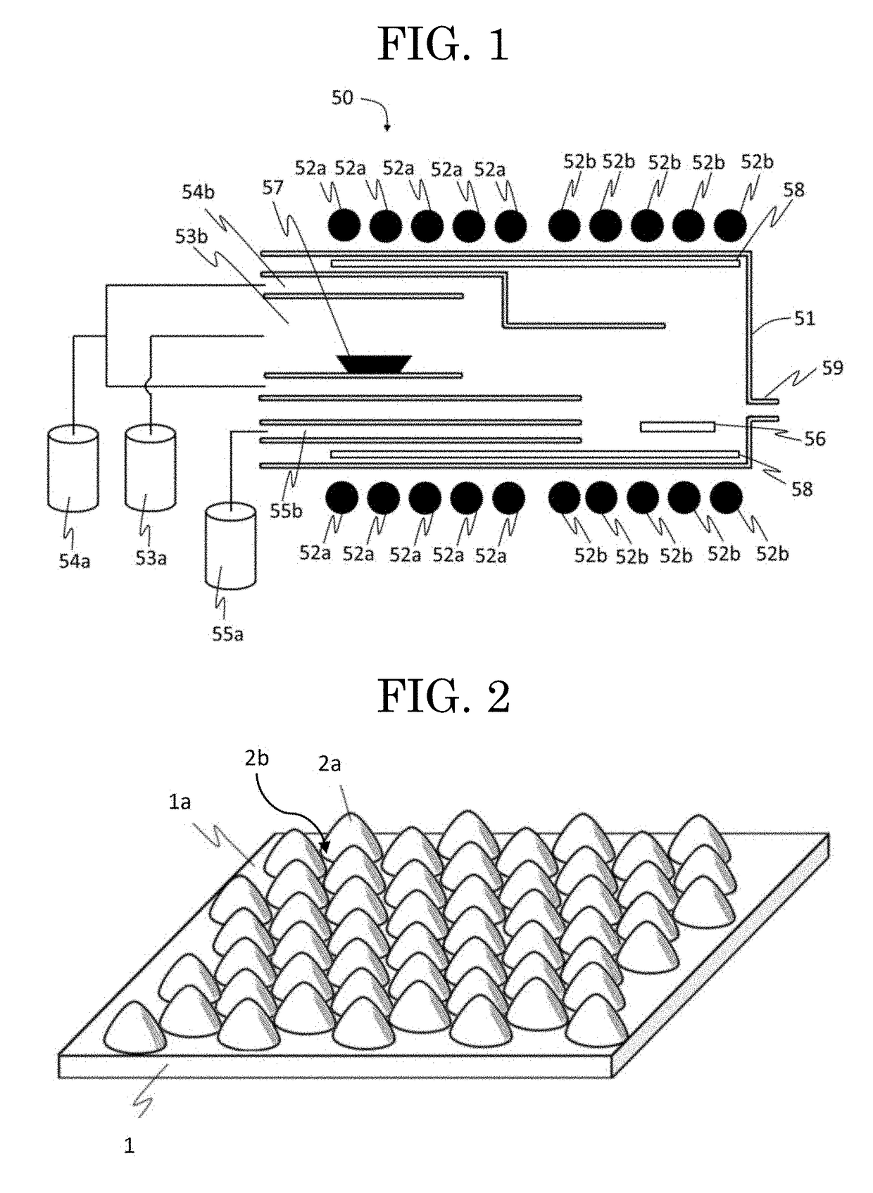
[0114]As an embodiment of a method of forming a crystalline layer, a mist chemical vapor deposition (CVD) method may be used. FIG. 8 shows a mist CVD apparatus 19 used in this embodiment. The mist CVD apparatus 19 includes a mist generator 24 with a container, and a vessel 25 containing water 25a, and an ultrasonic transducer 26 attached to a bottom of the vessel 25. The mist CVD apparatus 19 further includes a carrier gas supply 22a, and a flow-control valve of carrier gas 23a. Furthermore, the mist CVD apparatus 19 may include a dilution carrier gas supply device 22b, and a flow-control valve of dilution carrier gas 23b. The mist CVD apparatus 19 includes a film-formation chamber 27 that may be a quartz tube with an inner diameter of 40 mm, a heater 28, and a stand 21 to support an object 20 in the film-formation chamber 27. The heater 28 may be arranged at a periphery of the film-formation chamber 27. A film is to be formed on the object, and the ob...
example 2
[0131]A crystalline film was obtained by the same conditions as the conditions to form the crystalline film at Example 1 except the following six conditions: using a buffer layer arranged on an m-plane sapphire substrate that is without a pattern; arranging a sheet-shaped SiO2 mask including two or more openings on the buffer layer on the m-plane sapphire substrate; forming the crystalline film on the buffer layer and the SiO2 mask on the buffer layer; setting the film-formation temperature to 540° C.; setting the film-formation time to 120 minutes; and setting the flow gas rate of O2 to 10 sccm.
[0132]The two or more islands of crystalline metal oxide at the two or more openings of the SiO2 mask on the buffer layer of the substrate are grown. In this embodiment, the two or more islands of the crystalline metal oxide coalesce to form an epitaxial lateral overgrowth layer of the crystalline metal oxide and finally form the crystalline film.
[0133]FIG. 10A shows a perspective SEM image ...
PUM
 Abstract
Description
Claims
Application Information
 - R&D Engineer
- R&D Manager
- IP Professional
- Industry Leading Data Capabilities
- Powerful AI technology
- Patent DNA Extraction
Browse by: Latest US Patents, China's latest patents, Technical Efficacy Thesaurus, Application Domain, Technology Topic, Popular Technical Reports.
© 2024 PatSnap. All rights reserved.Legal|Privacy policy|Modern Slavery Act Transparency Statement|Sitemap|About US| Contact US: help@patsnap.com