Eureka AIR delivers breakthrough ideas for toughest innovation challenges, trusted by R&D personnel around the world.

Method for producing a nitride semiconductor crystal layer, nitride semiconductor crystal layer and substrate for producing the same

Inactive Publication Date: 2005-11-03
NAGOYA UNIVERSITY
View PDF17 Cites 3 Cited by
  • Summary
  • Abstract
  • Description
  • Claims
  • Application Information

AI Technical Summary

Benefits of technology

[0025] In the present invention, the AlN micro crystalline layer can be formed by means of any kind of forming method. Preferably the AlN micro crystalline layer can be formed through a lattice-shaped mask which is provided on the silicon substrate. In this case, the AlN micro crystalline layer is grown in the openings of the mask, embedding the openings and being formed uniformly. According to the forming method using the mask, the lattice distortion and the thermal expansion coefficient difference against the silicon substrate can be compensated, and the selective and lateral growth of the AlN micro crystalline layer can be realized in good condition. As a result, the AlN micro crystalline layer with high crystal quality can be easily formed thicker, e.g., in a thickness of 200 nm or over.
[0027] The mask can be made of at least one selected from silicon nitride, silicon dioxide and tungsten nitride. In this case, if the mask is held under a temperature and gas atmosphere in the formation of the nitride semiconductor crystal layer and the AlN micro crystalline layer, the mask can not be deteriorated and chemically reacted with the silicon substrate, the AlN micro crystalline layer and the nitride semiconductor crystal layer, so that the intended nitride semiconductor crystal layer can be formed precisely and stably and the crystal quality of the nitride semiconductor crystal layer can be enhanced sufficiently.

Problems solved by technology

However, the sapphire substrate (wafer) and the silicon carbide substrate (wafer) are expensive and the large-scaled sapphire substrate and the large-scaled silicon carbide substrate can not be almost available, so that the production cost of the compound semiconductor can not be reduced through the large scale of the substrate to be employed.
In this case, however, the large-scaled substrate can not be almost available and the peeling technique can not be established sufficiently.
With the above-mentioned conventional technique, however, the thickened nitride semiconductor film can not be formed.
When the silicon substrate and the nitride semiconductor crystal layer are held under a high temperature, however, the surface of the nitride semiconductor crystal layer may be roughed, so that the intended semiconductor element such as a semiconductor laser can not be fabricated by using the nitride semiconductor crystal layer.
With the HVPE method, a hydrochloric acid gas, which is generated through the chemical dissociation of raw material gases, promotes the chemical reaction between the nitride semiconductor crystal layer and the silicon substrate, but after the growth duration of one hour or over, the surface of the nitride semiconductor crystal layer is roughed and the nitride semiconductor crystal layer itself may be partially destroyed.
In order to enhance the performance of the optical element and reduce the production cost, it is required to develop the thickening growth technique of the nitride semiconductor crystal layer on the large-scaled silicon substrate, but such a thickening growth technique as mentioned above has not been developed yet.

Method used


Image

  • Method for producing a nitride semiconductor crystal layer, nitride semiconductor crystal layer and substrate for producing the same
  • Method for producing a nitride semiconductor crystal layer, nitride semiconductor crystal layer and substrate for producing the same
  • Method for producing a nitride semiconductor crystal layer, nitride semiconductor crystal layer and substrate for producing the same

Examples


example 1

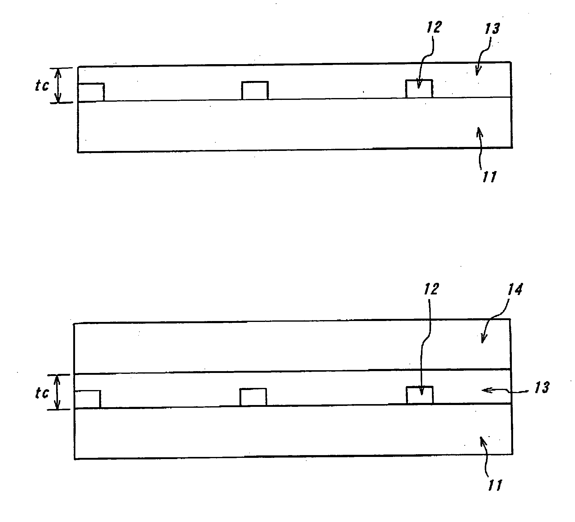
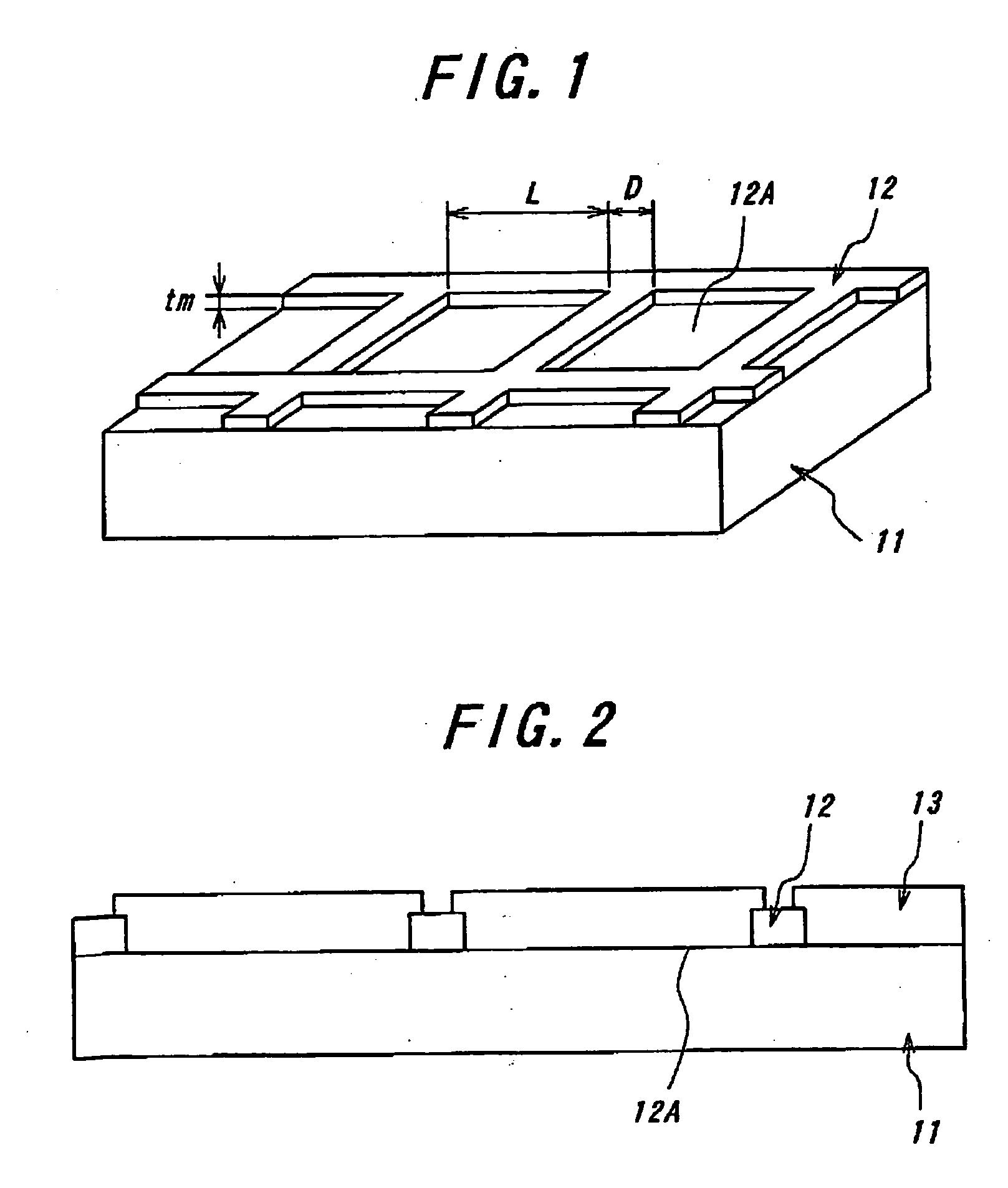
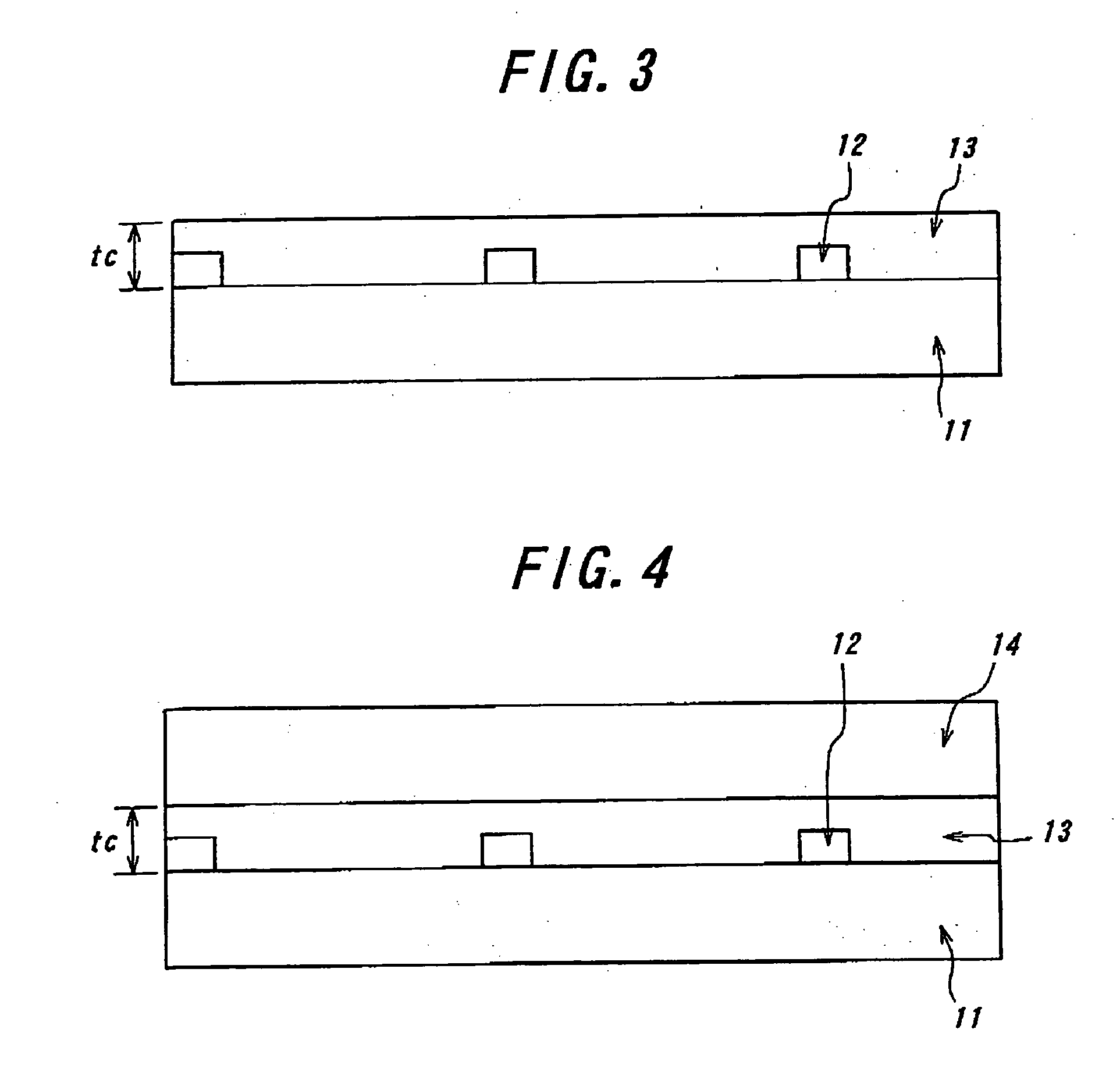
[0046] A GaN single crystal layer was formed by means of an MOCVD method on the steps as shown in FIGS. 1-4. Herein, the thickness tm of the mask Was set to 100 nm, and the length of each opening of the mask was set to 300 μm, and the distance between the adjacent openings, i.e., the pitch of the openings was set within 5-10 μm. The AlN micro crystalline layer 12 was formed in a thickness of 200 nm by heating the silicon substrate to 1000° C. by means of an MOCVE method. In this Example, the GaN single crystal layer was able to be thickened to a thickness of 1 μm or more during a growth period of 20 minutes. It was also confirmed by means of SEM observation that the surface of the GaN single crystal layer was extremely flat.

example 2

[0047] A GaN single crystal layer was formed by means of an HVPE method on the steps as shown in FIGS. 1-4. Herein, the same mask was employed as in Example 1, and an AlN micro crystalline layer 14 was formed in the same manner as in Example 1. In this Example, the GaN single crystal layer was able to be thickened to a thickness of about 40 μm at a substrate temperature of about 1000° C. during a growth period of two hours. It was also confirmed by men of SEM observation that the surface of the GaN single crystal layer was extremely flat.


PUM

PropertyMeasurementUnit
Temperatureaaaaaaaaaa
Lengthaaaaaaaaaa
Thicknessaaaaaaaaaa

Abstract

A mask with rectangular openings is formed on a large-scaled silicon substrate, and an AlN micro crystalline layer is formed in a thickness of 200 nm or over through the mask on the silicon substrate by means of selective and lateral growth. Then, a nitride semiconductor crystal layer with a composition of InxGayAlzN (0≦x, y, z≦1, x+y+z=1) is formed on the AlN micro crystalline layer.

Description

BACKGROUND OF THE INVENTION [0001] 1. Field of the Invention [0002] This invention relates to a method for producing a nitride semiconductor crystal layer, the nitride semiconductor crystal layer and a substrate for producing the nitride semiconductor crystal layer. [0003] 2. Description of the Related Art [0004] As of now, in the formation of a compound semiconductor with a composition of InxGayAlzN (0≦x, y, z≦1, x+y+z=1), a substrate made of sapphire (Al2O3) or silicon carbide (SiC) is prepared, and the intended compound semi-conductor is layered on the substrate by means of epitaxial growth. However, the sapphire substrate (wafer) and the silicon carbide substrate (wafer) are expensive and the large-scaled sapphire substrate and the large-scaled silicon carbide substrate can not be almost available, so that the production cost of the compound semiconductor can not be reduced through the large scale of the substrate to be employed. [0005] In the research and development of a nitri...

Claims


Application Information

Patent Timeline
IPC IPC(8): C23C16/34H01L21/20H01L21/205C30B29/38
CPCH01L21/02381H01L21/02458H01L21/02647H01L21/0262H01L21/02642H01L21/0254
Inventor SAWAKI, NOBUHIKOHONDA, YOSHIONISHIMURA, YOSHIYUKI
Owner NAGOYA UNIVERSITY
Why Eureka
Eureka Blog
Learn More