Spin orbit torque magnetoresistive random access memory containing composite spin hall effect layer including beta phase tungsten

a random access memory and spin orbit torque technology, applied in the field of spin orbit torque (sot) magnetoresistive memory cells, can solve the problems of neighboring cells being erroneously written, scalding these devices to high densities, and the current required to generate sufficient field to switch the free layer becomes prohibitively larg

Active Publication Date: 2019-03-14
SANDISK TECH LLC
View PDF1 Cites 35 Cited by
  • Summary
  • Abstract
  • Description
  • Claims
  • Application Information

AI Technical Summary

Problems solved by technology

Significant problems arise when scaling these devices to high densities.
Particularly, the currents required to generate sufficient field to switch the free layer become prohibitively large, and disturbances to neighboring cells or elements can occur during writing, which in turn may cause a neighboring cell to be erroneously written.

Method used


Image

  • Spin orbit torque magnetoresistive random access memory containing composite spin hall effect layer including beta phase tungsten
  • Spin orbit torque magnetoresistive random access memory containing composite spin hall effect layer including beta phase tungsten
  • Spin orbit torque magnetoresistive random access memory containing composite spin hall effect layer including beta phase tungsten

Examples


Embodiment Construction

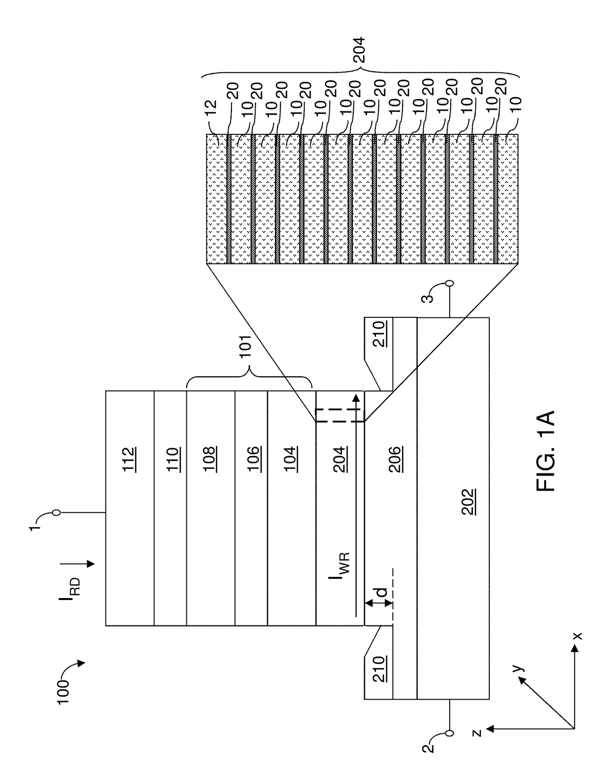
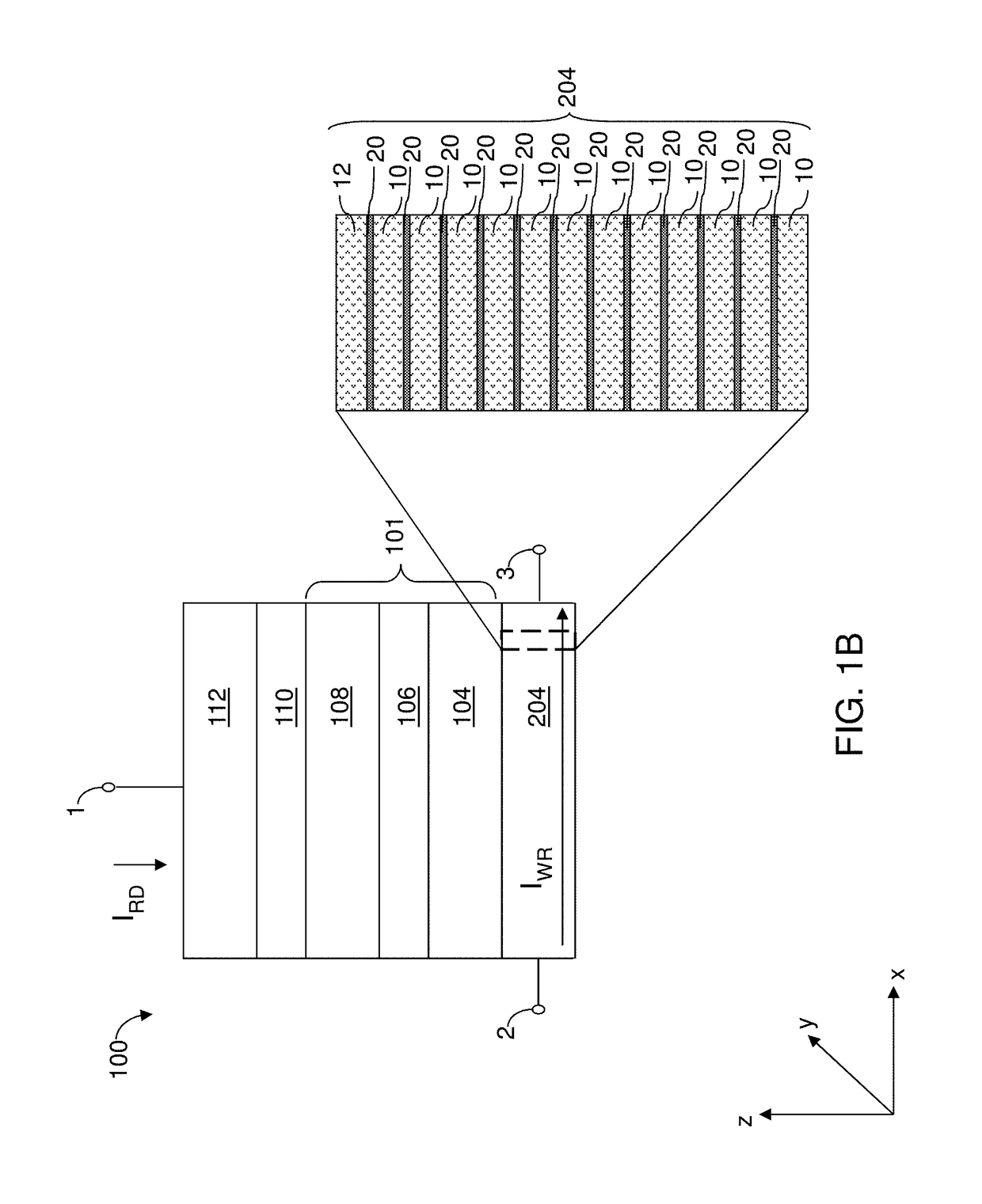
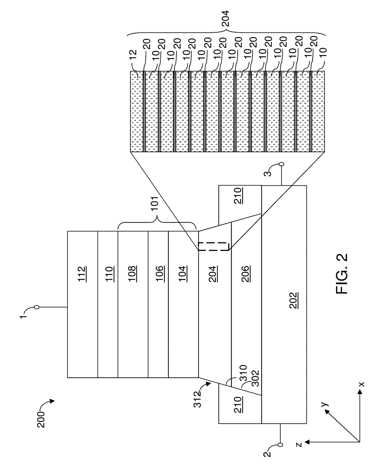
[0020]As discussed above, the present disclosure is directed to spin orbit torque (SOT) magnetoresistive memory cells, a random access memory device employing the same, and methods of manufacturing the same, the various aspects of which are described below. The embodiments of the disclosure can be employed to form various semiconductor devices such as three-dimensional memory array devices comprising MRAM devices. The drawings are not drawn to scale. Multiple instances of an element may be duplicated where a single instance of the element is illustrated, unless absence of duplication of elements is expressly described or clearly indicated otherwise. Ordinals such as “first,”“second,” and “third” are employed merely to identify similar elements, and different ordinals may be employed across the specification and the claims of the instant disclosure.

[0021]As used herein, a “layer” refers to a material portion including a region having a thickness. A layer may extend over the entirety ...


PUM


Abstract

A spin orbit torque magnetoresistive random access memory (SOT MRAM) cell includes a magnetic tunnel junction that contains a free layer having two bi-stable magnetization directions, a reference magnetic layer having a fixed magnetization direction, and a tunnel barrier layer located between the free layer and the reference layer, and a nonmagnetic spin Hall effect layer. The spin Hall effect layer may include an alternating stack of beta phase tungsten layers and noble metal nonmagnetic dusting layers. Alternatively or in addition, a hafnium layer may be located between the nonmagnetic spin Hall effect layer and the free layer.

Description

FIELD[0001]The present disclosure relates generally to the field of magnetic storage elements, and particularly to spin orbit torque (SOT) magnetoresistive memory cells.BACKGROUND[0002]Magnetoresistive random access memory (MRAM) is a non-volatile random-access memory technology. Unlike conventional random access memory (RAM), data in MRAM devices are not stored as electric charge or current flows. Instead, data is stored by magnetic storage elements. MRAM devices include cells or elements having a magnetically hard layer (i.e., a “reference” layer) and a magnetically soft layer (i.e., the “free” layer). Writing to MRAM is performed by passing current through current leads that are formed on either side of each memory element in order to create a local induced magnetic field, which sets the direction of the soft layer magnetization. Significant problems arise when scaling these devices to high densities. Particularly, the currents required to generate sufficient field to switch the ...

Claims


Application Information

Patent Timeline
Patent Type & Authority Applications(United States)
IPC IPC(8): G11C11/16G11C11/18H01L43/10H01L43/08H01L43/06H01L43/04
CPCG11C11/161G11C11/18H01L43/10G11C11/1673H01L43/06H01L43/04G11C11/1675H01L43/08G11C11/14G11C11/16G11C11/38H10N50/80H10N50/10H10N50/85H10N52/00H10N52/80
Inventor CHOI, YOUNG-SUKYORK, BRIANSMITH, NEIL
Owner SANDISK TECH LLC
Why Eureka
Try Eureka