HIGH CURRENT LATERAL GaN TRANSISTORS WITH SCALABLE TOPOLOGY AND GATE DRIVE PHASE EQUALIZATION

a gallium nitride transistor, high current technology, applied in the direction of electronic switching, semiconductor/solid-state device details, pulse techniques, etc., can solve the problems of unstable operation, poor performance, and introduction of significant parasitic on-chip inductance, and achieve the effect of improving the gate drive phase equalization and high current handling capacity

Active Publication Date: 2019-03-14
GAN SYST
View PDF0 Cites 10 Cited by
  • Summary
  • Abstract
  • Description
  • Claims
  • Application Information

AI Technical Summary

Benefits of technology

[0021]The present invention seeks to provide improved performance in devices and systems comprising GaN power transistors, particularly large area, high current lateral GaN power transistors, by balancing switching times of parallel transistor elements.

Problems solved by technology

In large area GaN transistors, for example, a device having an area of ˜1 cm2 or more, i.e. a die size of about 10 mm×10 mm, the length of on-chip wiring or interconnect tracks extending between the gate driver circuitry and gate electrodes of a large area GaN transistor can introduce significant parasitic on-chip inductances.
Unbalanced gate inductances may lead to unbalanced and unstable operation, and hence, poor performance.
Another consideration is that, when multiple GaN transistors are interconnected, or when multiple GaN transistor elements or sections of large area devices are connected in parallel, they are prone to current imbalance due to differences in parasitic resistances / inductances resulting from differing lengths of interconnect metallization for the gate drive signals.
Current imbalance is likely to occur during the turn-on rise time of switching transistors, due to lack of resistance balance.
However, on a cold start, during turn-on, the resistances of different transistor cells are not the same, due to fabrication imperfections in large scale GaN transistors.
However, reducing gate resistance adds to transistor gain and increases the likelihood of oscillations at the gate pin.
Increasing gate resistance adds to switching losses and reduces the efficiency of the transistor.

Method used


Image

  • HIGH CURRENT LATERAL GaN TRANSISTORS WITH SCALABLE TOPOLOGY AND GATE DRIVE PHASE EQUALIZATION
  • HIGH CURRENT LATERAL GaN TRANSISTORS WITH SCALABLE TOPOLOGY AND GATE DRIVE PHASE EQUALIZATION
  • HIGH CURRENT LATERAL GaN TRANSISTORS WITH SCALABLE TOPOLOGY AND GATE DRIVE PHASE EQUALIZATION

Examples


Embodiment Construction

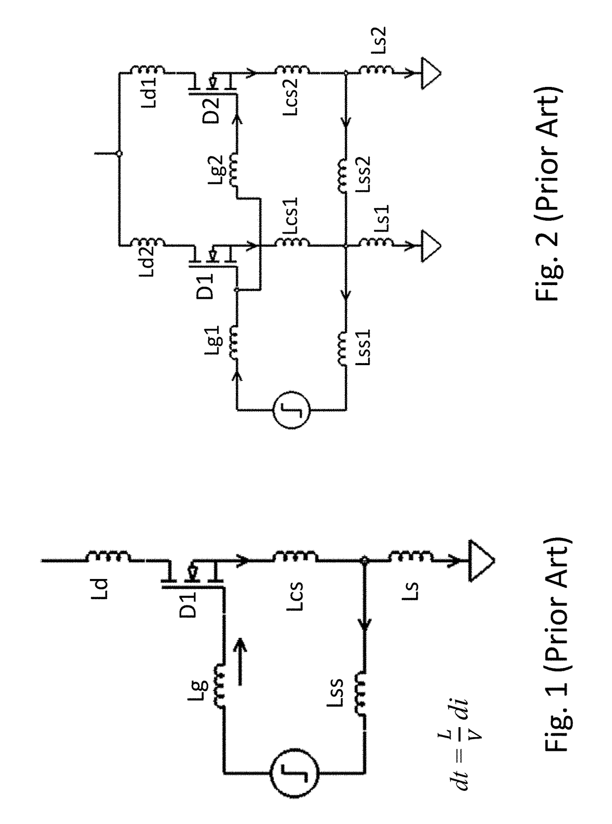
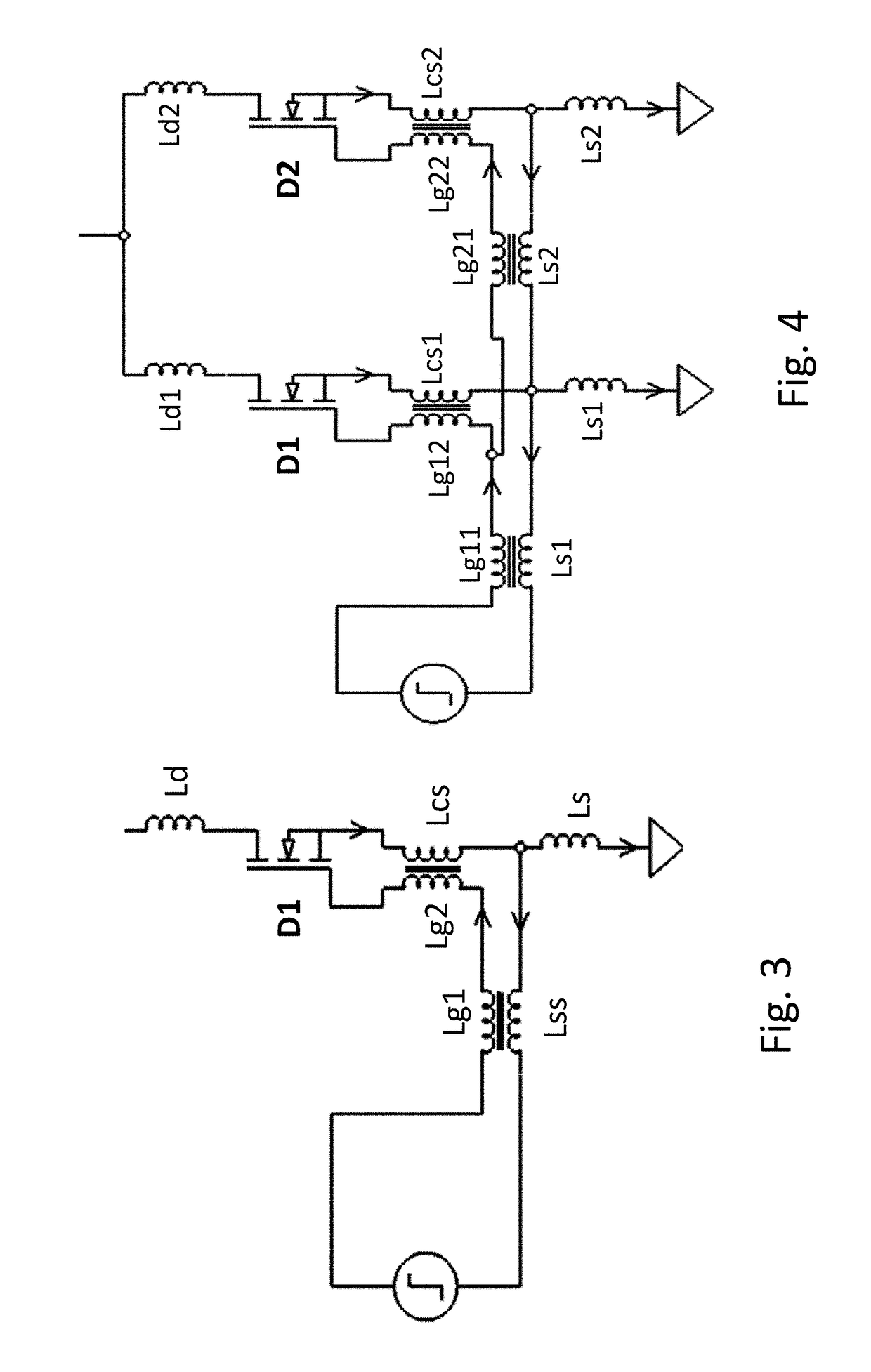
[0060]A circuit schematic of a lateral GaN transistor D1 connected to a gate drive supply voltage is shown in FIG. 1 (Prior Art) to illustrate parasitic inductances of the gate loop. That is, the gate delay is directly proportional to the total loop inductances dt=L / V di. The gate loop inductance includes the inductance of the gate drive path Lg, inductance of the gate return path Lss and the common source inductance Lcs. The drain inductance Ld and source inductance Ls in the power loop is also shown; the latter may include package interconnect inductances.

[0061]When two transistors are interconnected in parallel, for example as shown in the circuit schematic of FIG. 2 (Prior Art) comprising two a large area lateral GaN transistor elements D1 and D2 interconnected in parallel to a single gate drive supply voltage, it will be apparent that the difference in length of conductive tracks for each transistor element means that the gate loop inductance for the second transistor D2 (i.e. ...


PUM


Abstract

Large area, high current, lateral GaN power transistors are implemented using an on-chip interconnect topology wherein the transistor is arranged as an array of sections, each section comprising a set of transistor islands; gate and source buses that form each gate drive loop have substantially the same track widths; the source bus runs over or under the gate bus, and the tracks are inductively coupled to provide flux cancellation in the gate drive loop, thereby reducing parasitic inductances. The gate delay in each gate drive loop is reduced, minimizing the gate drive phase difference across the transistor. An overlying current redistribution layer preferably has a track width no greater than that of the underlying source and drain buses, for efficient coupling. This topology provides improved scalability, enabling fabrication of multi-section, large scale, high current lateral GaN transistors with reduced gate drive loop inductance, for improved operational stability.

Description

CROSS-REFERENCE TO RELATED APPLICATION(S)[0001]N / ATECHNICAL FIELD[0002]This invention relates to devices and systems comprising high current lateral gallium nitride (GaN) transistors, such as GaN power switches; it relates particularly to gate drive phase equalization and current redistribution for GaN High Electron Mobility Transistors (GaN HEMTs).BACKGROUND ART[0003]Large area, lateral GaN transistors for high voltage / high current operation, such as GaN power switches comprising GaN E-HEMTs, may comprise a plurality of transistor elements connected in parallel. For example, the topology of a large area, large gate width GaN E-HEMT may comprise a plurality of transistor elements in the form of islands which are interconnected in parallel. Each island comprises individual source, drain and gate electrodes and a plurality of islands are interconnected to form a multi-island transistor. Various topologies are known for large area transistors. Examples having an overlying interconnect ...

Claims


Application Information

Patent Timeline
Patent Type & Authority Applications(United States)
IPC IPC(8): H03K17/081H01L29/20H01L29/205H01L29/778H01L29/06H01L23/528H01L23/522
CPCH03K17/08104H01L29/2003H01L29/205H01L29/7787H01L23/3171H01L23/5283H01L23/5227H01L23/5286H01L29/0696H01L29/7786H01L23/4824H01L2224/49111H01L2224/48227H01L23/53228
Inventor MIZAN, AHMADKLOWAK, GREG P.CUI, XIAODONG
Owner GAN SYST
Why Eureka
Try Eureka