
Insulated-gate semiconductor device and method of manufacturing the same

a semiconductor device and gate-insulating film technology, applied in semiconductor devices, electrical equipment, transistors, etc., can solve the problems of low susceptibility to damage of gate-insulating film allocated at trench bottom, etc., to reduce the strength of electric field, avoid increase in on-resistance, and enhance the tolerance to short-circuit failure

Active Publication Date: 2019-05-09
FUJI ELECTRIC CO LTD
View PDF1 Cites 14 Cited by
  • Summary
  • Abstract
  • Description
  • Claims
  • Application Information

AI Technical Summary

Benefits of technology

The present invention provides an insulated-gate semiconductor device and a method of manufacturing it that can relax the strength of an electric field applied to the gate-insulating film and prevent an increase in on-resistance while enhancing its tolerance to short-circuit failures.

Problems solved by technology

Nevertheless, a disadvantage of such trench gate MOSFETs, which are made of a wide-bandgap semiconductor such as silicon carbide (SiC), is that a gate-insulating film allocated at a trench bottom is susceptive to damages ascribable to a higher voltage being applied to the gate-insulating film.
However, the semiconductor device disclosed in WO 2017 / 064949 A has low tolerance to a short-circuit failure because of a presence of a junction field-effect transistor (JFET) interposed between the first base region and the second base region on both sides of the respective trenches.

Method used


Image

  • Insulated-gate semiconductor device and method of manufacturing the same
  • Insulated-gate semiconductor device and method of manufacturing the same
  • Insulated-gate semiconductor device and method of manufacturing the same

Examples


first embodiment

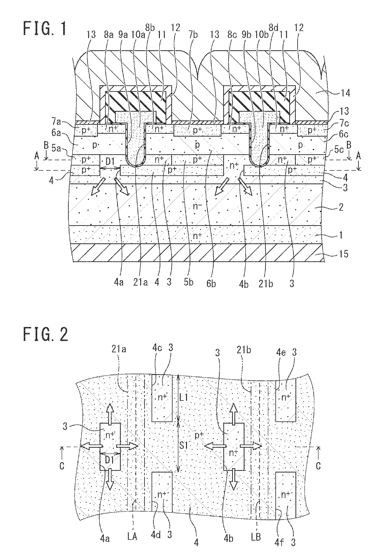
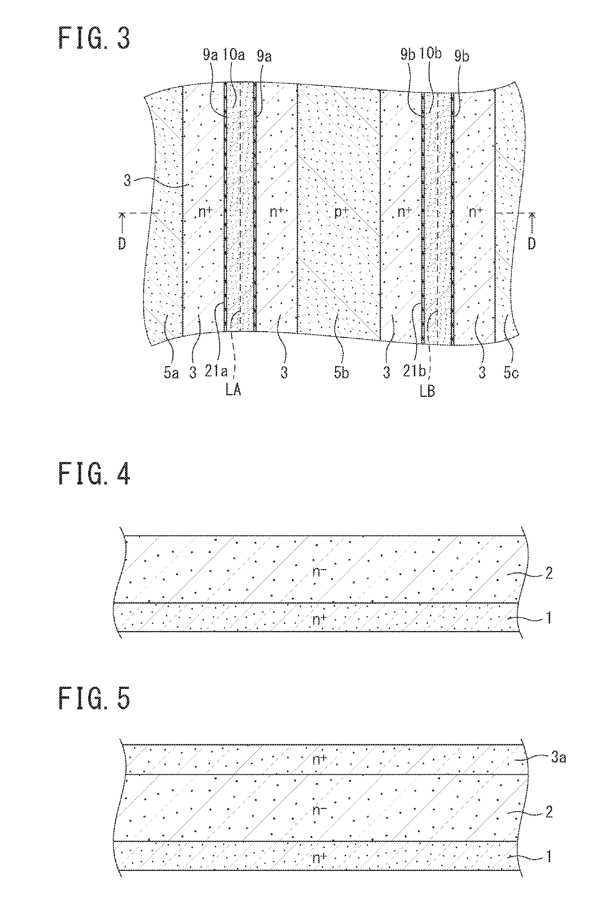
[0036]An insulated-gate semiconductor device, which is a metal-insulator-semiconductor field-effect transistor (MISFET), according to a first embodiment of the present invention includes a drift layer 2 of a first conductivity type (n-type), and a current spreading layer (CSL) 3 of n+-type having a higher impurity concentration than the drift layer 2 and disposed on the top surface of the drift layer 2, as illustrated in FIG. 1. The CSL 3 includes an upper-layer extending-part selectively extending in a horizontal direction and a lower-layer main-part parallel to the upper-layer extending-part so as to implement an L-shaped hook illustrated in the cross-sectional view of FIG. 1, and connecting parts connecting the upper-layer extending-part and the lower-layer main-part in a vertical direction. The drift layer 2 and the CSL 3 are each an epitaxially-grown layer (hereinafter simply referred to as an “epitaxial layer”) made of silicon carbide (SiC).

[0037]Base regions 6a, 6b, and 6c of...

second embodiment

Modified Example of Second Embodiment

[0075]FIG. 18 and FIG. 19 illustrate an insulated-gate semiconductor device according to a modified example of the second embodiment. FIG. 19 is a planar pattern at the horizontal level of the gate-bottom protection-region 4 as viewed from direction G-G in FIG. 18. FIG. 18 is a cross-sectional view as viewed from direction H-H in FIG. 19. As illustrated in FIG. 18 and FIG. 19, the insulated-gate semiconductor device according to the modified example of the second embodiment differs from the insulated-gate semiconductor device according to the second embodiment illustrated in FIG. 16 and FIG. 17 in that the width D1 of the openings 4a, 4b, 4c, 4d, 4e, and 4f, which are cut in the gate-bottom protection-region 4, is wider so that the gate-bottom protection-region 4 does not completely cover the bottoms of the trenches 21a and 21b. As illustrated in FIG. 19, the gate-bottom protection-region 4 and the openings 4a, 4b, 4c, 4d, 4e, and 4f may be arran...


PUM


Abstract

An insulated-gate semiconductor device includes: an n+-type current spreading layer disposed on an n−-type drift layer; a p-type base region disposed on the current spreading layer; a n+-type main-electrode region arranged in an upper portion of the base region; an insulated-gate electrode structure provided in a trench; and a p+-type gate-bottom protection-region being in contact with a bottom of the trench, including a plurality of openings through which a part of the current spreading layer penetrates, being selectively buried in the current spreading layer, wherein positions of the openings cut on both sides of a central line of the trench are shifted from each other about the central line in a longitudinal direction of the trench in a planar pattern.

Description

CROSS-REFERENCE TO RELATED APPLICATION[0001]This application claims benefit of priority under 35 USC 119 based on Japanese Patent Application No. 2017-214982 filed on Nov. 7, 2017, the entire contents of which are incorporated by reference herein.BACKGROUND OF THE INVENTION1. Field of the Invention[0002]The present invention relates to an insulated-gate semiconductor device having an insulated-gate electrode structure inside a trench, and a method of manufacturing the insulated-gate semiconductor device.2. Description of the Related Art[0003]Trench gate metal-oxide-semiconductor field-effect transistors (MOSFETs) are promising for a decrease in on-resistance with a reduction of a cell pitch, as compared with planar gate MOSFETs. Nevertheless, a disadvantage of such trench gate MOSFETs, which are made of a wide-bandgap semiconductor such as silicon carbide (SiC), is that a gate-insulating film allocated at a trench bottom is susceptive to damages ascribable to a higher voltage being ...

Claims


Application Information

Patent Timeline
Patent Type & Authority Applications(United States)
IPC IPC(8): H01L29/78H01L29/16H01L29/739H01L29/08
CPCH01L29/7813H01L29/1608H01L29/7397H01L29/086H01L29/0696H01L29/66348H01L29/1095H01L29/0623H01L29/66068H01L29/0878H01L29/0882H01L29/66734
Inventor KINOSHITA, AKIMASAOONISHI, YASUHIKOOKUMURA, KEIJI
Owner FUJI ELECTRIC CO LTD
Learn More