Single lamination blind and method for forming the same

Inactive Publication Date: 2019-05-09
R&D CIRCUITS
View PDF3 Cites 1 Cited by
  • Summary
  • Abstract
  • Description
  • Claims
  • Application Information

AI Technical Summary

Benefits of technology

[0005]The present invention provides for a method of removing the stub from one via. This avoids using back-drilling or performing multi-laminates by a method of a single lamination buried via methodology employing a seed layer resisted to prevent an electrical connection during electro-plating thus preventing the via from metalizing w

Problems solved by technology

There is a portion of the via that is extraneous and that

Method used


Image

  • Single lamination blind and method for forming the same
  • Single lamination blind and method for forming the same
  • Single lamination blind and method for forming the same

Examples


Embodiment Construction

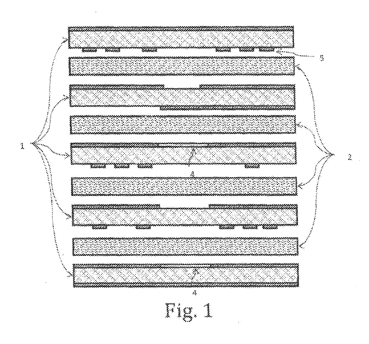
[0015]Referring now to FIGS. 1-9 of the drawings, FIG. 1 illustrates a common construction of a PCB before the individual layers are pressed together. A typical PCB is formed of multiple layers copper, copper clad core (1) and a partially cured dielectric also known as pre-preg (2). A seed-resist material (4) is deposited on two layers. FIG. 1 shows a common construction of a PCB before the individual layers have been pressed together. A typical PCB is made up of multiple layers of copper, copper clad core (1), and partially cured dielectric also known as pre-preg (2). Deposited on two layers is the seed-resist (4).

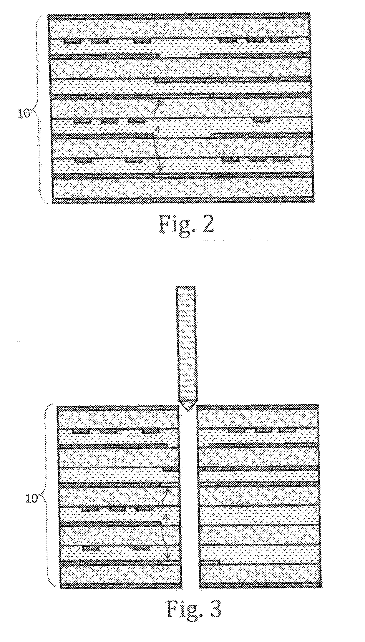
[0016]FIG. 2 shows the components in FIG. 1 after they have been laminated to form the PCB (10) or printed circuit board (10). FIG. 2 shows the components in FIG. 1 after they have been laminated. This forms the PCB (10) or circuit board.

[0017]FIG. 3 illustrates the drilling process for vias (9) formed in the PCB (10).

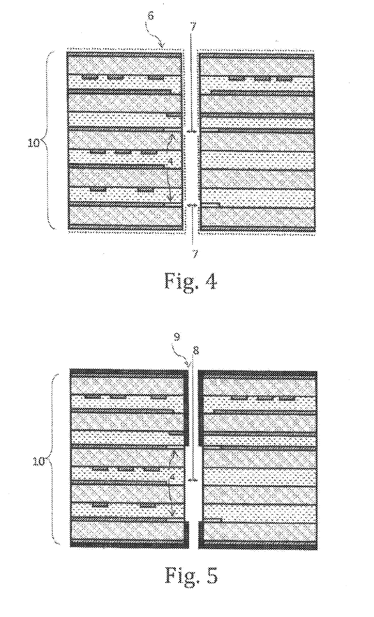
[0018]FIG. 4 shows deposition of a conductive layer us...


PUM


Abstract

A method and structure that forms a PCB while removing or eliminating a stub from a via without back-drilling or doing multi-laminations. In the preferred embodiment, the printed circuit board includes a via extending through a plurality of stacked layers. The via includes a plated through hole that is connected to at least two other metalized layers. There is a portion of the via that is extraneous and that has a negative performance on the functionality of the printed circuit board. The single lamination buried via method adds a seed layer resist that prevents an electrical connection during electroplating thus preventing the via from metalizing where it is not desired.

Description

RELATED APPLICATION[0001]The present non-provisional application claims priority to Provisional Application U.S. Ser. No. 62 / 541,307 filed on Aug. 4, 2017 by R&D Circuits, Inc. and claims priority thereunder pursuant to 35 U.S.C. 120.BACKGROUND OF THE INVENTION1. Field of the Invention[0002]The present invention relates to a structure and a method of removing a stub from a via without the need for back-drilling or to performing multi laminations. In particular, the present invention relates to a single lamination buried via method that adds a seed layer resist to prevent an electrical connection during electroplating which prevents the via from metalizing an undesired condition.2. The Related Art[0003]Printed Circuit Boards (PCBs) typically contain a plurality of vias, each of which electrically connects to a conductive trace on one layer of the PCB with one or more of the other layers of the PCB. Thus, illustratively, where a via interconnects two internal layers of the PCB, the po...

Claims


Application Information

Patent Timeline
IPC IPC(8): H05K3/42H05K3/46H05K1/11
CPCH05K3/429H05K3/4608H05K3/4611H05K3/427H05K3/422H05K3/423H05K1/115H05K3/0047H05K2203/072H05K2203/0723H05K2201/096H05K2201/09645H05K3/06H05K3/4623H05K2203/1415H05K2203/1423H05K2203/143
Inventor THOMPSON, DONALD ERICTURPUSEEMA, DHANANJAYA
Owner R&D CIRCUITS
Why Eureka
Try Eureka