Dynamic error handling for on-chip memory structures

a memory structure and dynamic error technology, applied in the field of integrated circuit architectures, can solve the problems of undesirable increase in the size of transistors, limited maximum speed of high-performance processors, and inability to handle errors, so as to improve the on-chip memory structure, improve the efficiency of error handling, and improve the effect of on-chip memory structur

Active Publication Date: 2016-04-26
WISCONSIN ALUMNI RES FOUND
View PDF13 Cites 0 Cited by
  • Summary
  • Abstract
  • Description
  • Claims
  • Application Information

AI Technical Summary

Benefits of technology

[0009]The present invention provides an improved on-chip memory structure that controls the activation of error handling bits as a function of operating voltage. In this way, error correction can be used to offset errors only when the memory structure is run at low voltage (and frequency). Consequently, negative performance impacts for evaluating error handling bits, such as additional access latencies, are avoided when the memory operates at higher voltage (and frequency) and memory errors are less likely.
[0010]In some embodiments, increased latencies due to evaluating error handling bits, such as correcting code (ECC) bits, redundant or backup memory bits, etc., may be hidden by reading digital data bits from memory structures speculatively and assuming no errors. Subsequently, in the background, the error handling bits may be evaluated for presence of errors in the digital data bits.
[0011]In some embodiments, certain portions of the memory structure may have larger cells, and therefore larger areas, than other portions. This, in turn, may provide not only higher reliability at low operating voltages, but also faster operation with reduced latency. As a result, for workloads or threads of execution not requiring as much resources or capacity, but preferring reduced access latency or cycle times at high voltage / frequency, the larger portions can be activated while the smaller portions are deactivated to improve performance.

Problems solved by technology

The maximum speed of high-performance processors is often limited by problems of power dissipation which may be addressed by improving energy efficiency.
Increasing the size of these transistors, however, is undesirable because memory structures typically occupy significant physical areas on integrated circuits.

Method used


Image

  • Dynamic error handling for on-chip memory structures
  • Dynamic error handling for on-chip memory structures
  • Dynamic error handling for on-chip memory structures

Examples


Embodiment Construction

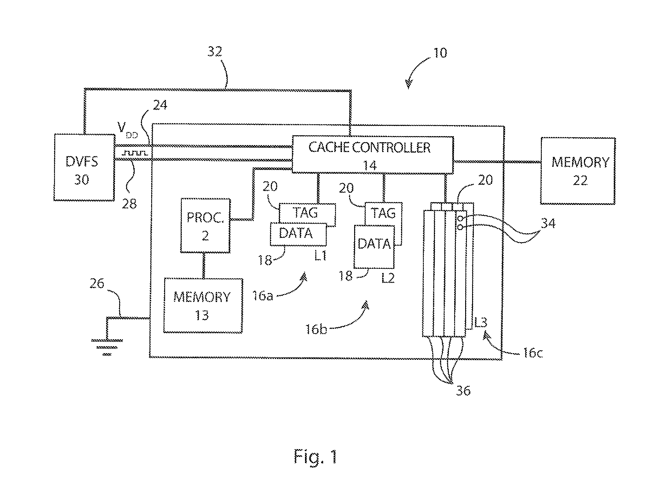
[0040]In an exemplar embodiment, referring now to FIG. 1, an integrated circuit element 10, for example, a core of a microprocessor or a freestanding microprocessor, may include a processor element 12 with memory structures such as a PRF, BTB, TLB, ROB, IQ, and LSQ. The processor element 12 may communicate with other memory structures and controllers, such as a scratchpad memory 13 and a cache controller 14 with an L1 cache 16a, an L2 cache 16b, and L3 cache 16c.

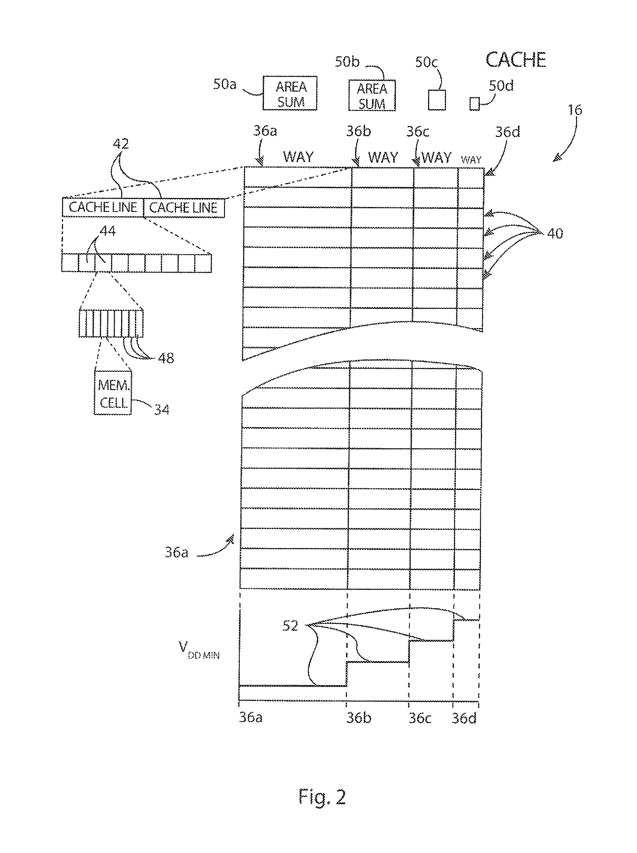
[0041]Each cache 16 may include a data portion 18 and tag portion 20 as is generally understood in the art, and operating under the control of the cache controller 14, may load data from a main memory 22 together with a tag address identifying the source address of that loaded data in the main memory 22, and may provide that loaded data to the processor element 12 in response to instructions reading the main memory 22 at the particular source address. The caches 16 may further receive modifications of the loaded data from t...


PUM


Abstract

A memory structure is provided that controls the activation of error handling bits as a function of operating voltage. In this way, error correction can be used to offset errors when the memory structure is run at low voltage (and frequency). However, negative performance impacts for such error correction, such as additional access latencies, can be avoided when the memory structure is run at higher voltage (and frequency) and memory errors are less likely. In addition, increased latencies due to evaluating error handling bits may be hidden by reading digital data bits from the memory structures speculatively and assuming no errors. Also, certain portions of memory structures may have larger cells, and therefore larger areas, than other portions, which may provide not only higher reliability at low operating voltages, but also faster operation with reduced latency.

Description

STATEMENT REGARDING FEDERALLY SPONSORED RESEARCH OR DEVELOPMENT[0001]This invention was made with government support under 1016262 awarded by the National Science Foundation. The government has certain rights in the invention.BACKGROUND OF THE INVENTION[0002]The present invention relates to architectures for integrated circuits, and, in particular, to improved methods and apparatuses providing reliable and power conserving, low-voltage operation of memory structures.[0003]Current computer architectures employ various types of memory structures, such as caches and static random access memories (SRAM); scratchpad memories, or high-speed internal memories used for temporary storage of calculations, data, and other work in progress; dynamic random access memories (DRAM); physical register files (PRF); branch target buffers (BTB); translation look-aside buffers (TLB); re-order buffers (ROB); instruction queues (IQ); load / store queues (LSQ); and so forth. These memory structures serve a v...

Claims


Application Information

Patent Timeline
Patent Type & Authority Patents(United States)
IPC IPC(8): G11C29/00G06F11/10G11C7/00G11C5/14G11C29/52G11C29/04
CPCG11C29/52G06F11/1076G11C5/147G11C2029/0409G11C2029/0411
Inventor KIM, NAM SUNG
Owner WISCONSIN ALUMNI RES FOUND
Why Eureka
Try Eureka