Method for manufacturing semiconductor

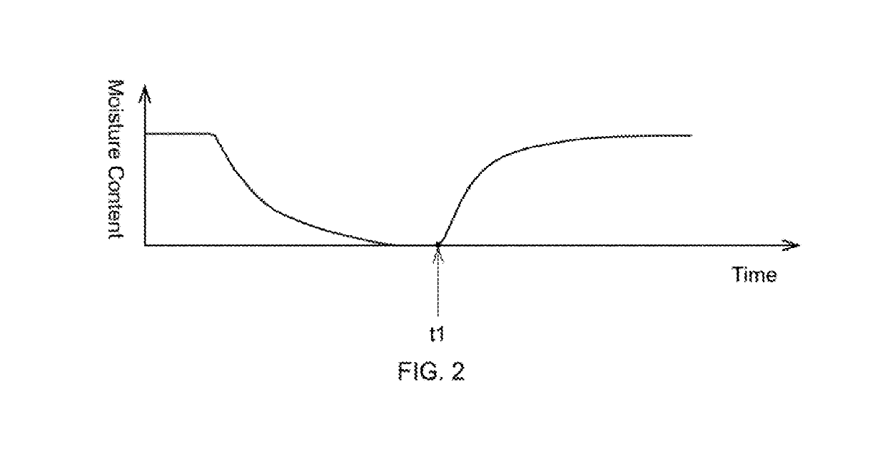
a manufacturing method and semiconductor technology, applied in the field of semiconductor manufacturing, can solve the problems of increasing the humidity or oxygen concentration of the humidity in the foup, the difficulty of managing small dust in the entire clean room, and the cost of the whole process, so as to prevent and suppress the rapid increase in the humidity or oxygen concentration, and avoid the effect of quality degradation due to the moisture adhered on the wafer

Inactive Publication Date: 2019-05-16
SINFONIA TECHNOLOGY CO LTD
View PDF4 Cites 2 Cited by
  • Summary
  • Abstract
  • Description
  • Claims
  • Application Information

AI Technical Summary

Benefits of technology

[0016]The EFEM thus configured can perform purging leading to a high maximum concentration of a predetermined gaseous atmosphere by the bottom purge apparatus so as to maintain a low humidity at or below a predetermined value in the purge container. Even when the internal space of the purge container is in communication with that of the wafer transport chamber, a gas curtain that shields the opening of the load port can be formed by the shield gas curtain apparatus to prevent and suppress the entrance of the gaseous atmosphere in the wafer transport chamber into the purge container. Consequently, even after the internal space of the purge container is in communication with that of the wafer transport chamber, a low humidity can be maintained in the purge container and a rapid increase in the humidity in the purge container can be avoided. According to the EFEM of the present invention, which is capable of thus maintaining a low humidity in the purge container, adherence of moisture onto a wafer in the purge container can be prevented and suppressed, and quality degradation due to the moisture adhered on a wafer can be avoided.
[0017]Even when a gas curtain is formed by the shield gas curtain apparatus provided in the EFEM according to the present invention, it is conceivable that the humidity in the purge container may somewhat increase after the internal space of the purge container is brought into communication with that of the wafer transport chamber from the level at that time. The increased humidity, however, will reach a peak at some point in time and the peak level will be smaller than the case where a gas curtain is not formed by the shield gas curtain apparatus, which is small enough to prevent and suppress adherence of moisture onto a wafer. In view of this point, according to the EFEM of the present invention, during a process of bottom purging to reduce the humidity in the purge container with the bottom purge apparatus while the internal space of the purge container is not in communication with that of the wafer transport chamber, wafer transportation can be started when the humidity reaches the same level as the above-described peak level by bringing the internal space of the purge container into communication with that of the wafer transport chamber. In this way, time needed from when bottom purging is started for the purge container to when the internal space of the purge container is brought into communication with that of the wafer transport chamber can be reduced, leading to tact time reduction, and consequently, an improved efficiency of wafer processing.
[0019]The load port has advantages similar to the EFEM. Specifically, it is possible to perform purging leading to a high maximum concentration of a gaseous atmosphere by the bottom purge apparatus so as to maintain a low humidity at or below a predetermined value in the purge container. Even when the internal space of the purge container is in communication with that of the wafer transport chamber, a gas curtain that shields the opening can be formed by the shield gas curtain apparatus to prevent and suppress the entrance of the gaseous atmosphere in the wafer transport chamber into the purge container. Consequently, even after the internal space of the purge container is in communication with that of the wafer transport chamber, a low humidity can be maintained in the purge container and a rapid increase in the humidity in the purge container can be avoided. According to the load port of the present invention, which is capable of thus maintaining a low humidity in the purge container, adherence of moisture onto a wafer in the purge container can be prevented and suppressed, and quality degradation due to the moisture adhered on a wafer can be avoided.
[0020]Even when a gas curtain is formed by the shield gas curtain apparatus provided in the load port according to the present invention, it is conceivable that the humidity in the purge container may somewhat increase after the internal space of the purge container is brought into communication with that of the wafer transport chamber from the level at that time. The increased humidity, however, will reach a peak at some point in time and the peak level will be smaller than the case where a gas curtain is not formed by the shield gas curtain apparatus, which is small enough to prevent and suppress adherence of moisture onto a wafer. In view of this point, according to the load port of the present invention, during a process of bottom purging to reduce the humidity in the purge container with the bottom purge apparatus while the internal space of the purge container is not in communication with that of the wafer transport chamber, wafer transportation can be started when the humidity reaches the same level as the above-described peak level by bringing the internal space of the purge container into communication with that of the wafer transport chamber. In this way, time needed from when bottom purging is started for the purge container to when the internal space of the purge container is brought into communication with that of the wafer transport chamber can be reduced, leading to tact time reduction, and consequently, an improved efficiency of wafer processing.
[0021]Furthermore, according to the EFEM and the load port of the present invention, a low oxygen concentration in the purge container can also be maintained, the oxygen being a cause of wafer oxidation.
[0023]According to the present invention, an EFEM and a load port can be provided, which include a bottom purge apparatus for bottom purging and a shield gas curtain apparatus that forms a gas curtain, and operate these apparatuses to prevent and suppress a rapid increase in the humidity or the oxygen concentration in a purge container occurring immediately after the internal space of the purge container is brought into communication with that of a wafer transport chamber, so that quality degradation due to the moisture adhered on a wafer can be avoided.

Problems solved by technology

Today, however, when the trends of high integration of devices and circuit miniaturization along with the adoption of larger wafers have progressed, it has become difficult to manage small dusts in an entire clean room in view of costs as well as from a technical point of view.
As miniaturization of semiconductor devices on a wafer or the like progresses, there is growing concern about quality degradation due not only to contamination but also to moisture adhered on a wafer in these days, leading to a necessity of keeping a clean and low humidity environment around wafers.
It has been found that when the lid of the FOUP is opened at the door section of the load port while a low humidity environment is maintained inside the FOUP, which is a purge container, once the bottom purging is performed to replace the atmosphere in the FOUP with the predetermined gas, the internal space of the FOUP is brought into communication with that of the wafer transport chamber through the opening of the load port, and the gaseous atmosphere in the wafer transport chamber enters the internal space of the FOUP, which may result in a rapid increase in the humidity in the FOUP.
Such a rapid increase in the humidity in the FOUP, which has once been reduced by the bottom purging down to a predetermined value or lower in order to secure a low humidity environment, may increase the possibility of moisture being adhered on a wafer and lead to a potential degradation of quality.
It has also been found that the oxygen concentration in the FOUP shows the same trend as the humidity; if the oxygen concentration in the FOUP increases when the lid of the FOUP is opened, an oxide film may disadvantageously be formed on the wafer.
However, since the front purging disclosed in Japanese Patent Laid-Open No. 2007-180516 can be performed only while the lid of the FOUP is opened at the door section of the load port, it has a disadvantage of a maximum concentration of gaseous atmosphere being lower than that reachable by the bottom purging.
Even though such a relatively lower maximum concentration of gaseous atmosphere can be maintained, a relatively higher maximum concentration of gaseous atmosphere, as can be reached by the bottom purging, cannot be maintained, so that it is not expected to completely eliminate the possibility of moisture being adhered on a wafer in the gaseous atmosphere in the FOUP, which leads to a potential degradation of quality.

Method used


Image

  • Method for manufacturing semiconductor
  • Method for manufacturing semiconductor
  • Method for manufacturing semiconductor

Examples


Embodiment Construction

[0031]A first embodiment of the present invention will now be described with reference to drawings.

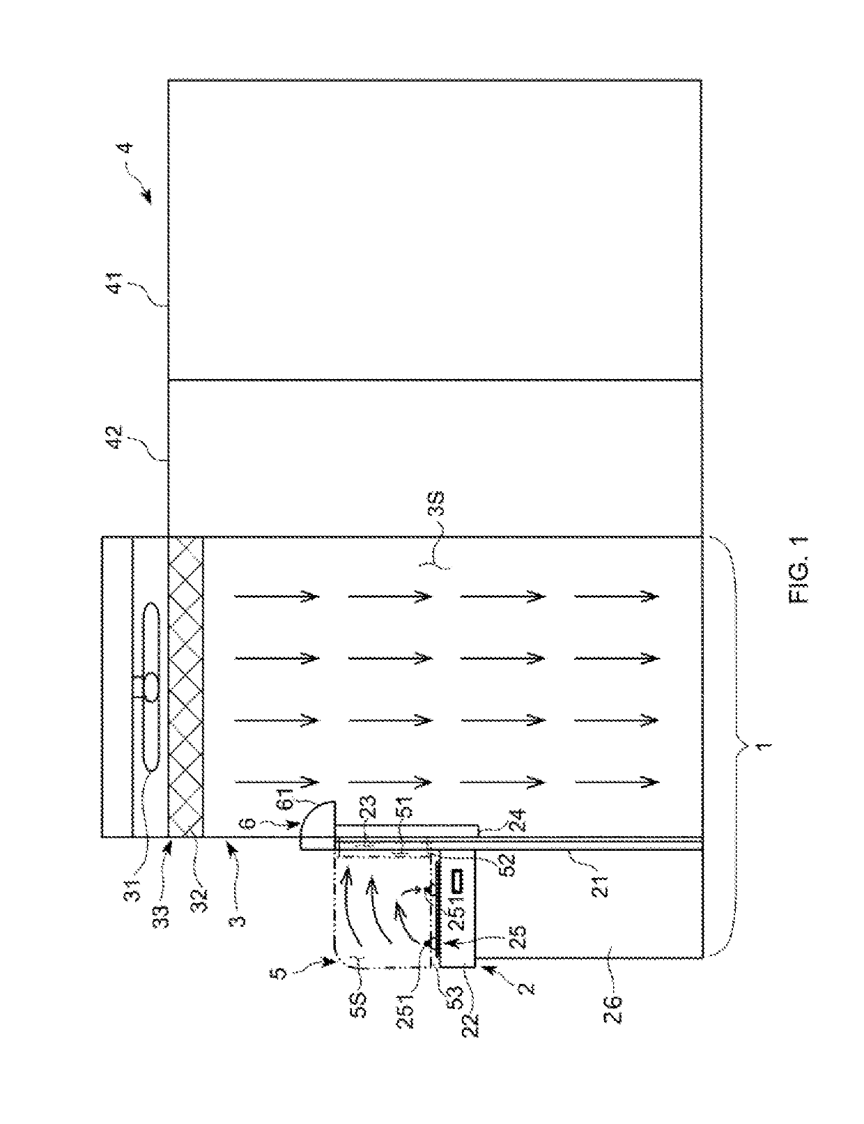
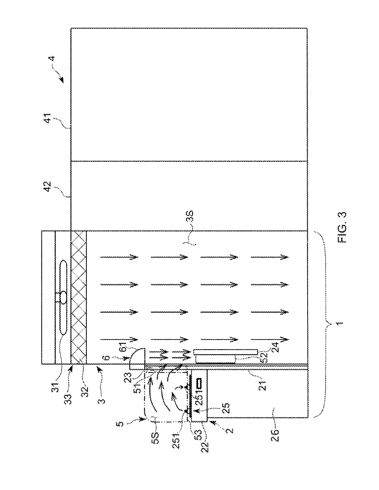
[0032]As illustrated in FIG. 1, an EFEM 1 according to the embodiment is composed of a load port 2 and a wafer transport chamber 3 adjacent to each other in a common clean room. FIG. 1 is a diagram of the load port 2 and its surroundings when viewed from one side, and schematically illustrates a relative positional relation of the load port 2 and the wafer transport chamber 3, as well as a relative positional relation of the EFEM 1, which is composed of the load port 2 and the wafer transport chamber 3, a semiconductor manufacturing apparatus 4, and a FOUP 5, which is a purge container.

[0033]The FOUP 5 illustrated by a long dashed double-short-dashed line in FIG. 1 houses a plurality of wafers therein, is configured to allow the wafers to be exchanged through a carrying-in / carrying-out port 51 formed in a front face, and includes a lid 52 capable of opening and closing the carrying-in / ...


PUM


Abstract

There is provided a method for manufacturing semiconductor. The method includes providing a semiconductor manufacturing apparatus and providing an EFEM. The EFEM includes a shield gas curtain apparatus 6 that forms a gas curtain capable of shielding an opening 23 when an internal space 5S of a purge container 5, in which the humidity is reduced to a predetermined value by means of a bottom purge apparatus 25 provided in a load port 2, is brought into communication with an internal space 3S of a wafer transport chamber 3, the gas curtain being formed of a shield curtain gas blown immediately downward from a location near the opening 23 of the load port 2 and being closer to the wafer transport chamber 3 than the opening 23 at a higher height than an upper edge of the opening 23.

Description

CROSS-REFERENCE TO RELATED APPLICATION[0001]The application is a Divisional of U.S. patent application Ser. No. 14 / 269,360, filed on May 5, 2014, which claims a priority of Japanese Application No. 2013-147207 filed on Jul. 16, 2013.BACKGROUND OF THE INVENTIONField of the Invention[0002]The present invention relates to an EFEM composed of a wafer transport chamber and a load port, and to a load port.Description of the Related Art[0003]In a semiconductor manufacturing process, wafers are processed in a clean room to improve yield and quality. Today, however, when the trends of high integration of devices and circuit miniaturization along with the adoption of larger wafers have progressed, it has become difficult to manage small dusts in an entire clean room in view of costs as well as from a technical point of view. Accordingly, instead of increasing the cleanliness of the entire interior of such a clean room, a system that incorporates “mini-environment system,” which locally increa...

Claims


Application Information

Patent Timeline
Patent Type & Authority Applications(United States)
IPC IPC(8): F24F9/00H01L21/677H01L21/67
CPCF24F9/00H01L21/67772H01L21/67017F24F3/161F24F3/167H01L21/67763
Inventor TANIYAMA, YASUSHIOCHIAI, MITSUTOSHINATSUME, MITSUOSUZUKI, ATSUSHI
Owner SINFONIA TECHNOLOGY CO LTD
Why Eureka
Try Eureka