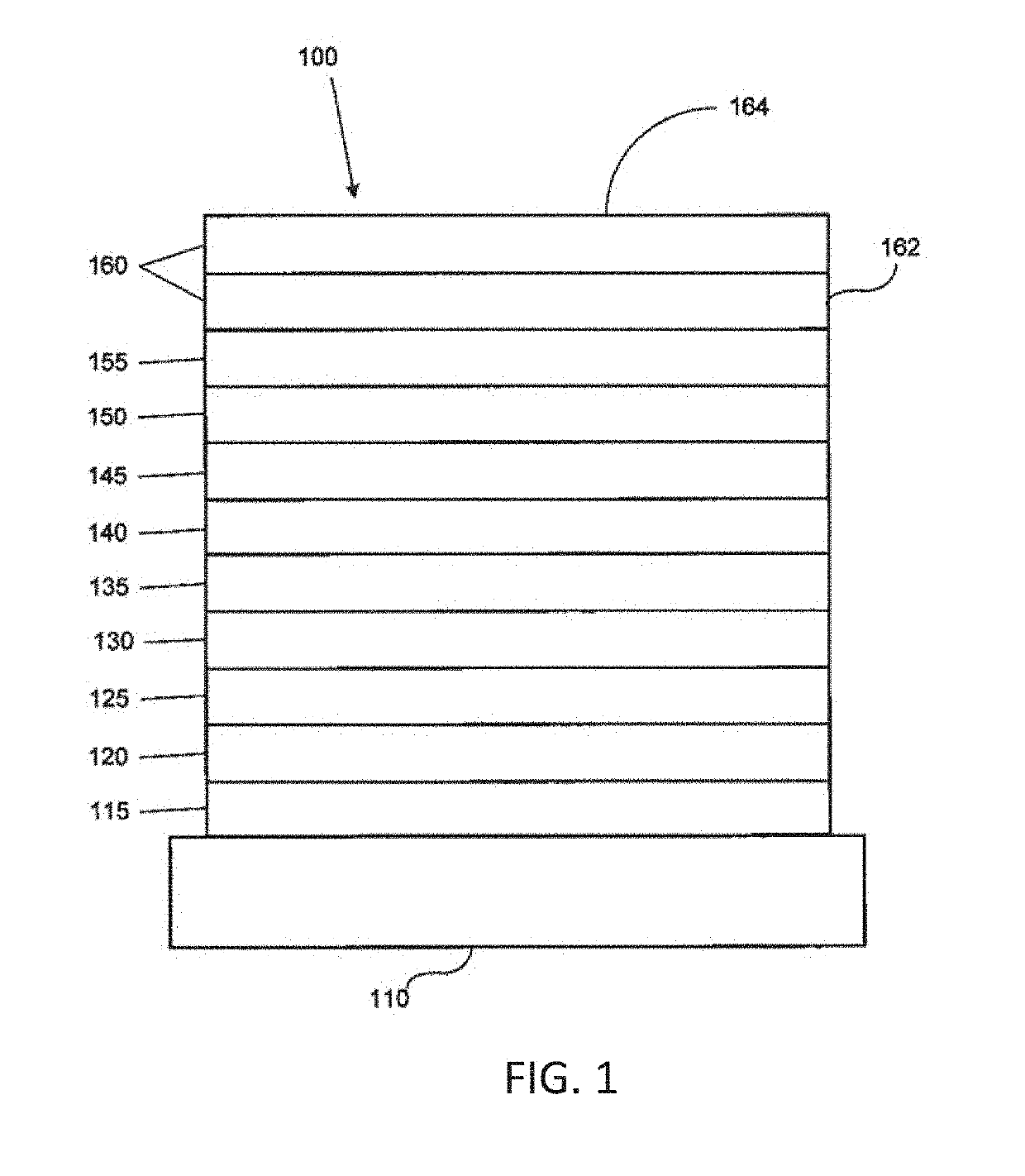
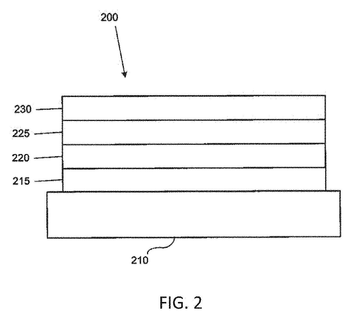
OLED with minimal plasmonic losses
a plasmonic loss and plasmonic light technology, applied in the field of oled with minimal plasmonic loss, can solve the problems of important and unsolved optical loss mechanism, loss of light output due to waveguide and spp modes, and loss of light output due to waveguide and spp modes, and achieve the effect of high refractive index
- Summary
- Abstract
- Description
- Claims
- Application Information
AI Technical Summary
Benefits of technology
Problems solved by technology
Method used
Image

Examples
Embodiment Construction
[0037]The term “transparent” is defined by a transmission of light of at least 80% through a subject material of a given thickness compared to a reference material of indium tin oxide of the same thickness set at 100% transmission.
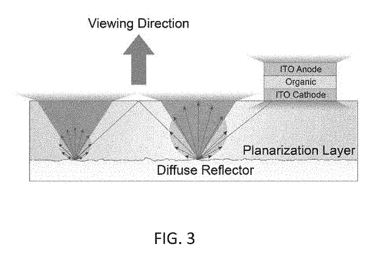
[0038]The total external quantum efficiency (EQE), which is the product of the internal quantum efficiency (IQE) and the outcoupling efficiency (ηout), is regarded as one of the critical parameters for a light-emitting device because it describes the amount of emitted photons (or light) per unit of electrical energy supplied to the device. As noted above, the inherent layered structure of OLEDs causes a low outcoupling efficiency since generated photons become trapped in waveguide modes and are wasted in the excitation of SPPs. For example, the external quantum efficiency (EQE) of current OLEDs lies around 20% with conventional glass substrates, i.e., in the absence of outcoupling enhancements.
[0039]It remains a challenge to develop a highly efficient outc...
PUM
 Abstract
Description
Claims
Application Information
 - R&D Engineer
- R&D Manager
- IP Professional
- Industry Leading Data Capabilities
- Powerful AI technology
- Patent DNA Extraction
Browse by: Latest US Patents, China's latest patents, Technical Efficacy Thesaurus, Application Domain, Technology Topic.
© 2024 PatSnap. All rights reserved.Legal|Privacy policy|Modern Slavery Act Transparency Statement|Sitemap