MEMS device for an implant assembly

a technology of an implanted sensor and a body, which is applied in the field of structure for implanted sensor packages, can solve the problems of slow changes in distance between, signal drift, and unfavorable experience of capacitance changes, and achieve the effects of reducing capacitive gap changes, and enhancing at least one performance parameter of said implan

Active Publication Date: 2019-05-23
ENDOTRONIX
View PDF0 Cites 0 Cited by
  • Summary
  • Abstract
  • Description
  • Claims
  • Application Information

AI Technical Summary

Benefits of technology

[0010]This application relates to hermetically packaged wireless electronics and more particularly to an implantable sensor design and manufacturing approach to optimize manufacturability, size, longevity, RF characteristics, and overall performance while minimizing potential effects of operating in various pressure conditions, temperature conditions and manufacturing induced stress conditions.
[0012]The at least one discontinuity may allow at least one electrical trace to connect at least one said electrical contact outside of said capacitive gap to at least one electrode positioned at least partially within said capacitive gap. The capacitive gap may include electrodes positioned on said diaphragm and said floating base. The implant may include a coil in electrical communication with said sensor, said coil positioned within said housing. The diaphragm may be made of a glass material and the floating base may be made of silicon. The diaphragm may include a thickness of about 195 μm and said at least one discontinuity may include a length of about 6.75 mm. The location and size of said at least one discontinuity may be configured to enhance at least one performance parameter of said implant. The at least one performance parameter may be selected from the following list: sensitivity to pressure, sensitivity to temperature, mechanical strength, and long term accuracy. Sensitivity to temperature may be improved by positioning said at least one discontinuity such that a coefficient of thermal expansion mismatch effect counteracts a gas expansion effect to reduce capacitive gap change due to temperature.
[0015]In yet another embodiment, provided is an implant that comprises a housing having a plurality of walls and at least one opening. A sensor may be connected to an opening in said housing, said sensor comprising a first layer having a first dimension and a second layer having a second dimension shorter than said first dimension. Said second layer may be positioned entirely within said housing and a surface of said first layer is exposed to the exterior of said housing. Said second layer may be attached to said first layer to define a capacitive gap between layers, said attachment being positioned along a perimeter of said capacitive gap. Said attachment along said perimeter may include at least one discontinuity. The location and position of said at least one discontinuity may be configured to enhance at least one performance parameter of said implant.

Problems solved by technology

Stress relaxation along the bond line may be a slow change over time which can cause signal drift due to slow change in capacitive gap height.
However, it is not desirable to also experience capacitance changes due to any other reason, including: slow changes in the composition of gas (or fluid) in the capacitive gap over time; slow changes in distance between plates due to relaxation of built-in internal stresses over time; and changes in temperature.
These composition changes may cause error in implant readings because capacitance (and hence resonant frequency) may be changing for reasons other than due to external pressure.
If, for example, a component within the implant housing (such as a PCB) outgasses water vapor into the housing cavity, and the vent between the housing cavity and capacitive gap is only a small hole, it may take a long time for the capacitive gap to achieve homogeneity with the outer housing cavity, causing long term inaccuracy while the stabilization (homogeneity) takes place.
Further challenges have been identified related to the practical implementation of such an implant.
These temperature and pressure variations may cause the sensor to communicate inconsistent signals or otherwise function in an inconsistent manner.
Further, because MEMS fabrication processes can be complex and require very long development times, it is desirable to identify designs that allow modifying performance specifications with only minor changes in structure.

Method used


Image

  • MEMS device for an implant assembly
  • MEMS device for an implant assembly
  • MEMS device for an implant assembly

Examples


Embodiment Construction

[0034]Reference will now be made in detail to embodiments of the invention, examples of which are illustrated in the accompanying drawings. It is to be understood that other embodiments may be utilized and structural and functional changes may be made without departing from the respective scope of the invention.

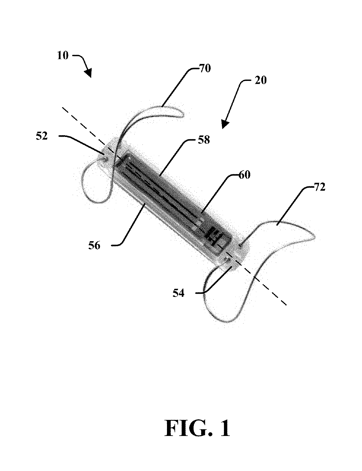
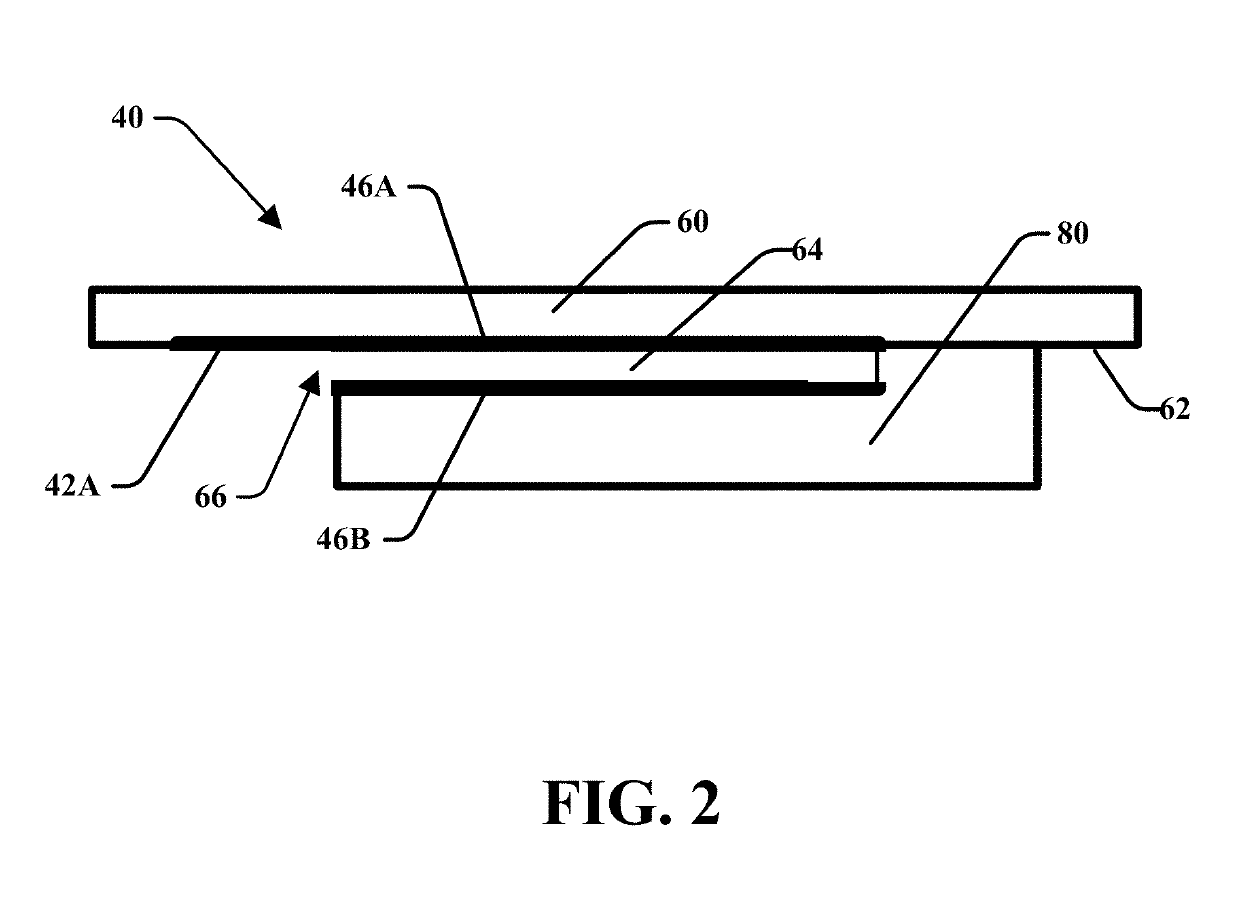
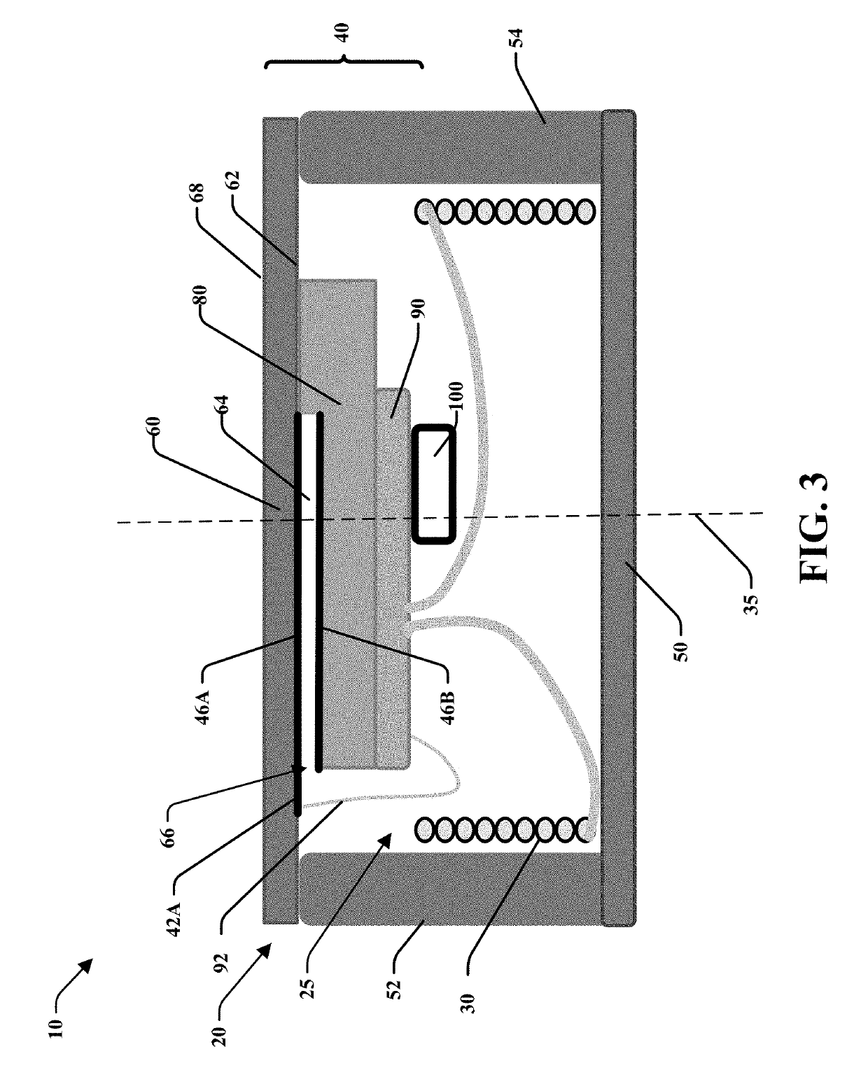
[0035]This application relates to an implant 10 and more particularly to an implantable sensor design and manufacturing approach to optimize manufacturability, size, longevity, RF characteristics, Q, and overall performance related to increasing sensitivity and minimizing thermally induced frequency offset. To improve the device design and to minimize thermally induced frequency offset, the implant may be constructed to optimize deflection of the surfaces of the implant capacitor while providing ample protection from the environment and maximizing space for the internal components such as the coil.

[0036]In one embodiment, the instant application refers to an improvement to th...


PUM


Abstract

Disclosed is an implant and method of making an implant. The implant having a housing that defines a cavity. The housing includes a sensor comprising a base attached to a diaphragm wherein said base may be positioned within said cavity. The sensor may be a capacitive pressure sensor. The diaphragm may be connected to the housing to hermetically seal said housing. The sensor may include electrical contacts positioned on the diaphragm. The attachment between the base and the diaphragm may define a capacitive gap and at least one discontinuity configured to enhance at least one performance parameter of said implant.

Description

CROSS-REFERENCE TO RELATED APPLICATIONS[0001]This application claims priority to and the benefit of each the following applications: U.S. Provisional Patent Application No. 62 / 618,848 entitled “MEMS DEVICE FOR AN IMPLANT ASSEMBLY,” filed on Jan. 18, 2018. This application is also a continuation-in-part of U.S. patent application Ser. No. 15 / 213,712 entitled “PRESSURE SENSING IMPLANT” filed on Jul. 19, 2016 which is a continuation-in-part of U.S. patent application Ser. No. 14 / 777,654 entitled “PRESSURE SENSING IMPLANT” filed on Sep. 16, 2015 which is a national phase entry application that claims priority to International Patent Application No. PCT / US2014 / 030661 filed Mar. 17, 2014 which claims priority to Provisional Patent Application No. 61 / 786,793 entitled “PRESSURE SENSING IMPLANT,” filed on Mar. 15, 2013. This application is also a continuation-in-part of U.S. patent application Ser. No. 15 / 837,075 entitled “IMPLANTABLE SENSOR ENCLOSURE WITH THIN SIDEWALLS,” filed on Dec. 11, ...

Claims


Application Information

Patent Timeline
Patent Type & Authority Applications(United States)
IPC IPC(8): A61B5/07A61B5/0215A61B5/145A61B5/03A61B5/00A61B5/01
CPCA61B5/076A61B5/0215A61B5/14503A61B5/036A61B5/0031A61B5/0059A61B5/01A61B2562/168A61B5/6869A61B5/6876A61B5/02152A61B5/08A61B2562/0247
Inventor ZAMAN, MOHAMMAD FAISALFONG, JEFFREYCHEE, JULIANPANIAN, TYLERNAGY, MICHAEL
Owner ENDOTRONIX
Why Eureka
Try Eureka