Flexible display panel and manufacturing method thereof

a flexible display and manufacturing method technology, applied in the direction of sustainable manufacturing/processing, identification means, instruments, etc., can solve the problems of abnormal display of flexible display panels, reduce the damage to inner devices and metal wiring film layers, and eliminate the erosion of film layers. , the effect of cost saving

Active Publication Date: 2019-05-30
WUHAN CHINA STAR OPTOELECTRONICS SEMICON DISPLAY TECH CO LTD
View PDF0 Cites 12 Cited by
  • Summary
  • Abstract
  • Description
  • Claims
  • Application Information

AI Technical Summary

Benefits of technology

[0007]The present disclosure provides a flexible display panel capable of efficiently improving a yield rate of the flexible display panels, eliminating erosion of film layers caused by electrostatic charges, and protecting the screen displayed by flexible driving panels from being damaged.
[0017]In the present disclosure, a series of capacitors are added to the empty region of the non-display region. The capacitors have an ability to buffer a release of electrostatic charges, thereby reducing the damage to inner devices and metal wiring film layers caused by the electrostatic charges and protecting the metal wiring film layers from being damaged and destroyed by the electrostatic charges during the manufacture of active thin-film transistors of the flexible display panel. This can efficiently improve a yield rate of the flexible display panels, eliminate erosion of the film layers caused by the electrostatic charges, and protect the screen displayed by flexible driving panels from being damaged. The first metal plate and the first gate electrode are formed using a same process as well as the second metal plate and the second gate electrode. It does not require additional processes, thereby achieving cost savings.

Problems solved by technology

However, during manufacturing, accumulated electrostatic charge can easily damage second gate electrodes in a fan-out area of a non-display region, resulting in erosion or damage of signal transmission lines, causing a display of a flexible display panel to be abnormal.

Method used


Image

  • Flexible display panel and manufacturing method thereof
  • Flexible display panel and manufacturing method thereof
  • Flexible display panel and manufacturing method thereof

Examples


Embodiment Construction

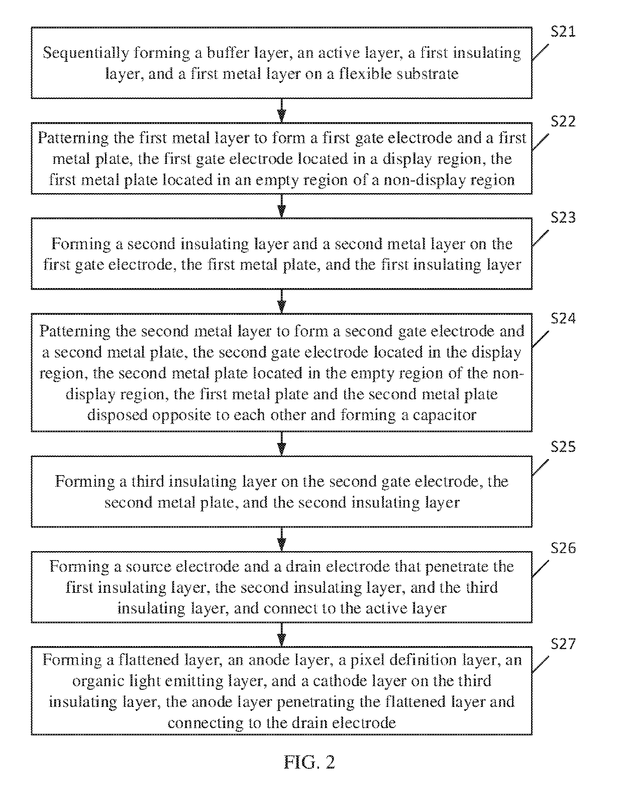
[0021]Embodiments of a flexible display panel provided in the present disclosure will be described in detail with reference to the appended figures.

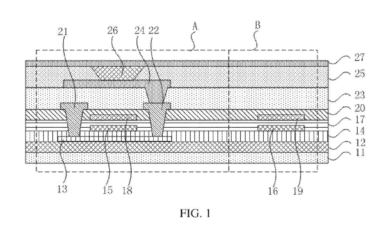
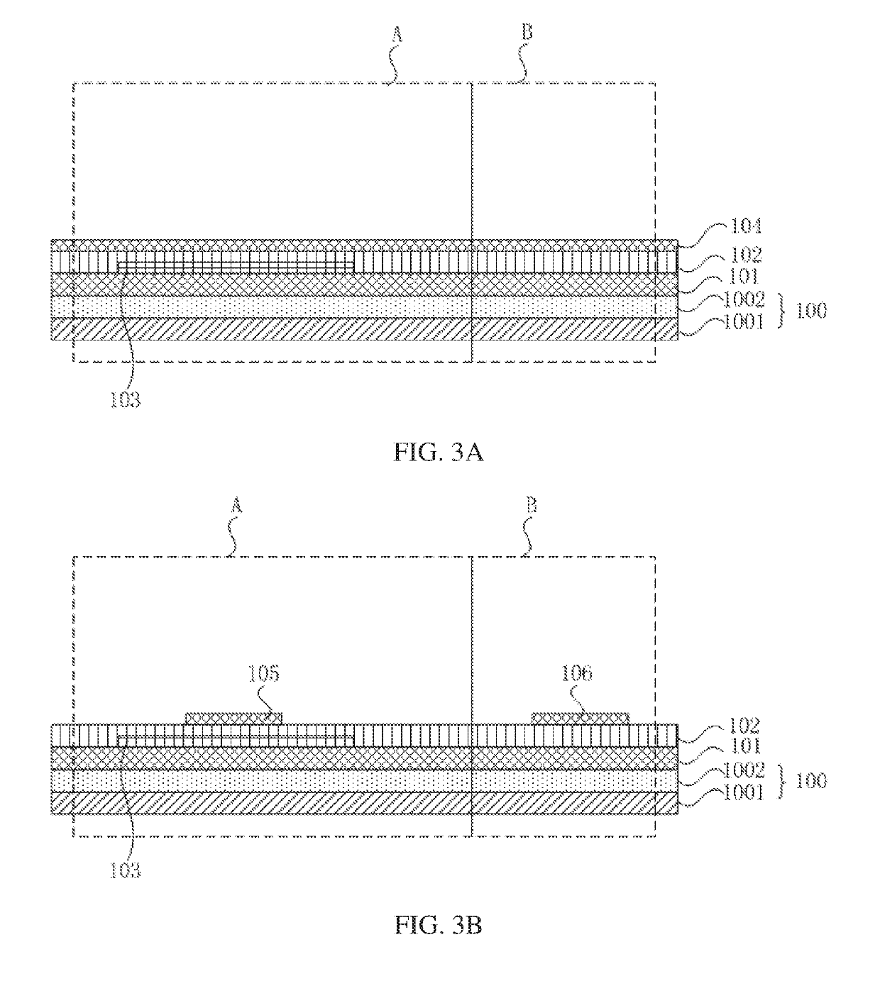
[0022]FIG. 1 is a schematic structural diagram showing a flexible display panel in accordance with the present disclosure. Referring to FIG. 1, the flexible display panel of the present disclosure includes a display region A and a non-display region B. In FIG. 1, the display region A and the non-display region B are denoted schematically with dashed boxes. The flexible display panel of the present disclosure is an organic light emitting diode (OLED) display panel, that is, an OLED flexible display panel. The display region A has organic light emitting diodes. The display region A is configured to display images. The non-display region B is a region outside the display region A, for example, metal wiring regions. In the non-display region B, the metal wiring regions are called a fan-out region. An empty region is located between the metal...


PUM


Abstract

A flexible display panel includes a display region and a non-display region. Capacitors are added to an empty region of the non-display region. The capacitors have ability to buffer a release of electrostatic charges, thereby reducing damage to inner devices and metal wiring film layers caused by the electrostatic charges and protecting the metal wiring film layers from being damaged and destroyed by the electrostatic charges during manufacturing active thin-film transistors of the flexible display panel.

Description

BACKGROUND1. Field of the Disclosure[0001]The present disclosure relates to display device technologies, and more particularly to a flexible display panel.2. Description of Related Art[0002]As a major base and carrier of information transfer and exchange, display devices, such as liquid crystal displays (LCDs) and organic light emitting diode (OLED) displays, are gaining more attention and are widely used in people's life, work, etc. In recent years, with increasing demand for portable display devices, flexible display technology has become one of the most competitive display technologies and has been favored by both industries and consumers. One great advantage of the flexible display technology is its foldability. This property can increase display area without increasing device size, and makes the device very portable. Flexible TFT-LCDs and flexible OLED displays have gradually developed into the most promising high-tech industries. Various types of flexible display devices, such...

Claims


Application Information

Patent Timeline
Patent Type & Authority Applications(United States)
IPC IPC(8): H01L27/32H01L51/00
CPCH01L27/3265H01L27/3262H01L51/0097H01L2227/323H01L27/1255H01L2251/5338H01L27/1288H01L29/78645G09F9/301H01L27/1214H10K59/12H01L27/1218Y02E10/549Y02P70/50H10K59/1216H10K77/111H10K59/1201H10K2102/311H10K59/1213
Inventor WANG, XING
Owner WUHAN CHINA STAR OPTOELECTRONICS SEMICON DISPLAY TECH CO LTD
Why Eureka
Try Eureka