Method for producing ge-core based waveguides

a technology of waveguides and ge-cores, applied in the field of methods, to achieve the effects of increasing the deposition speed of cladding materials, high atom mobility, and increasing the depositing speed

Active Publication Date: 2019-06-13
COMMISSARIAT A LENERGIE ATOMIQUE ET AUX ENERGIES ALTERNATIVES
View PDF0 Cites 1 Cited by
  • Summary
  • Abstract
  • Description
  • Claims
  • Application Information

AI Technical Summary

Benefits of technology

[0034]This low-temperature depositing avoids an increase that is too high in the mobility of atoms of the core at the level of the free surfaces. Yet, in the scope of the development of the present invention, it has been identified that the alteration of the core at least partially comes from this mobility that is too high of the atoms. This low-temperature depositing thus makes it possible to preserve a rectangular cross-section, for example, of the core of the waveguide. It avoids the appearance of faces and the alteration of the free surfaces linked to a redistribution of material of the core.
[0035]To increase the deposition speed of the cladding material around the core, so as to make the method compatible with an industrial production, the deposition of the “low-temperature” shell is followed by a “high-temperature” depositing of the encapsulation layer, at a temperature Tencapsulation epitaxy significantly higher than the deposition temperature of the shell Tshell epitaxy.
[0036]For example, the deposition by epitaxy temperature of the encapsulation layer Tencapsulation epitaxy is greater than or equal to 830° C. and preferably greater than or equal to 850° C., so as to benefit from increase depositing speeds.
[0037]The shell, being less germanium-rich than the core, is more robust than the core vis-à-vis this “high-temperature” depositing. The core is thus protected by the shell during the formation of the very thick cladding.

Problems solved by technology

A challenge is to produce such waveguides with an industrial yield.

Method used


Image

  • Method for producing ge-core based waveguides
  • Method for producing ge-core based waveguides
  • Method for producing ge-core based waveguides

Examples


Embodiment Construction

[0054]Before starting a detailed review of the embodiments of the invention, optional characteristics are stated below which can possibly be used in association or alternatively:

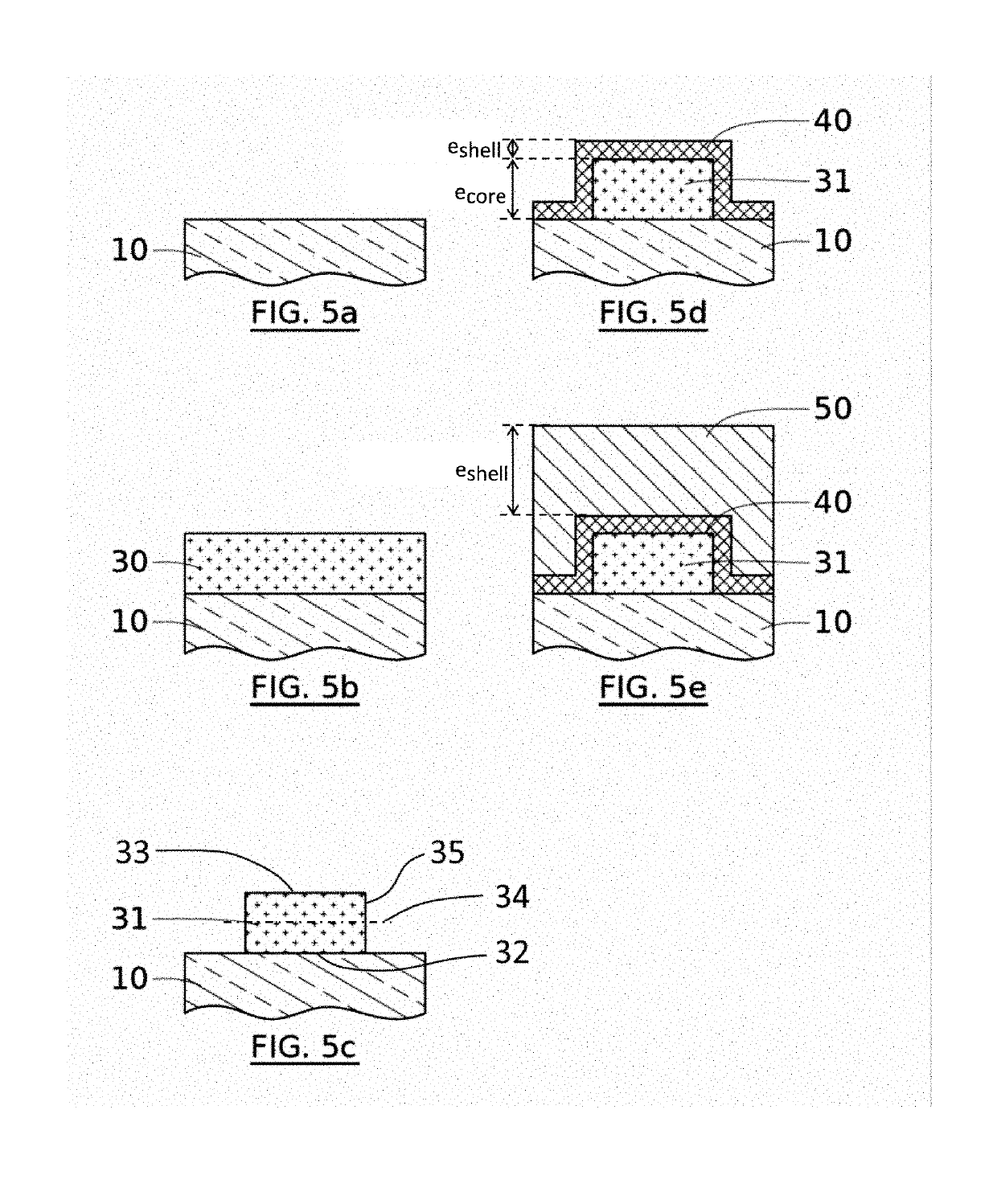
According to a particularly advantageous embodiment for producing waveguides optimized for light fluxes having wavelengths of between 3 μm and 8 μm (3-8 μm IRM band), the method can comprise the optional characteristics which can possibly be used in association or alternatively:[0055]the Ge-based layer is a silicon-germanium (SiGe) layer.[0056]the Ge-based layer has a thickness ecore of between 1 and 4 μm, the thickness ecore being determined along a direction perpendicular to the main plane wherein the substrate extends.[0057]the Ge-based layer has a substantially constant germanium content along the thickness ecore and is between 20% and 50%.[0058]alternatively to the preceding characteristic, the Ge-based layer has a varying germanium content along a direction perpendicular to the main plane wherein the s...


PUM

PropertyMeasurementUnit
thicknessaaaaaaaaaa
thicknessaaaaaaaaaa
thicknessaaaaaaaaaa

Abstract

A method for producing a waveguide including a germanium-based core and a cladding is provided, the method including a step of “low temperature” depositing of a shell after forming the core by engraving, such that the deposition temperature is less than 780° C., followed by a step of “high temperature” depositing of a thick encapsulation layer. The shell and the encapsulation layer at least partially form the cladding of the waveguide. Optionally, a step of annealing under hydrogen at a “low temperature”, less than 750° C., precedes the deposition of the shell. These “low temperature” annealing and depositing steps advantageously make it possible to avoid a post-engraving alteration of the free surfaces of the core during the forming of the cladding which is less germanium-rich.

Description

TECHNICAL FIELD OF THE INVENTION[0001]The invention relates to the field of optical waveguides. It has a particularly advantageous application in producing waveguides suitable for the infrared medium spectrum.STATE OF THE ART[0002]In the field of optical waveguides configured to confine and propagate a light flux having a wavelength belonging to the infrared medium (IRM) spectrum, a technology generally consists of producing a waveguide comprising a core and a cladding surrounding the core, the core and the cladding having a sufficiently high optical index contrast to confine the light flux in the core of the waveguide.[0003]In particular, for light flux wavelengths of between 3 μm and 8 μm (10−6 meters), such an IRM waveguide by index contrast can comprise a silicon-germanium (SiGe) core with a germanium concentration of a few tens of atomic percent, and a silicon (Si) cladding.[0004]For light flux wavelengths of between 8 μm and 15 μm, such an IRM waveguide by index contrast can c...

Claims


Application Information

Patent Timeline
Patent Type & Authority Applications(United States)
IPC IPC(8): C23C16/06G02B6/10C30B25/02C23C16/56C23C16/24
CPCC23C16/06G02B6/102C30B25/02C23C16/56C23C16/24G02B6/131H01L21/0245H01L21/02532H01L21/0262G02B2006/12061
Inventor HARTMANN, JEAN-MICHELBRUN, MICKAELFEDELI, JEAN-MARCFOURNIER, MARYSE
Owner COMMISSARIAT A LENERGIE ATOMIQUE ET AUX ENERGIES ALTERNATIVES
Why Eureka
Try Eureka