
Defect discovery using electron beam inspection and deep learning with real-time intelligence to reduce nuisance

a technology of deep learning and discovery of defects, applied in semiconductor/solid-state device testing/measurement, image enhancement, instruments, etc., can solve problems such as difficulty in deskew, take one to two days to find all defect types, and high nuisance ra

Active Publication Date: 2019-07-11
KLA TENCOR TECH CORP
View PDF0 Cites 9 Cited by
  • Summary
  • Abstract
  • Description
  • Claims
  • Application Information

AI Technical Summary

Benefits of technology

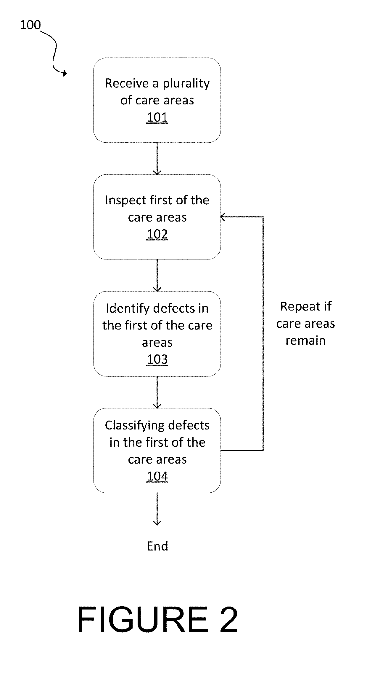
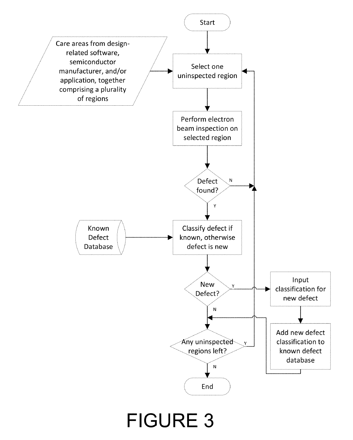
The present invention improves a wafer inspection tool by making better decisions to quickly find new defect types. This saves time by avoiding redundant inspection of the same area where a defect is already found. The inspection process can stop when all new and known defect types are found.

Problems solved by technology

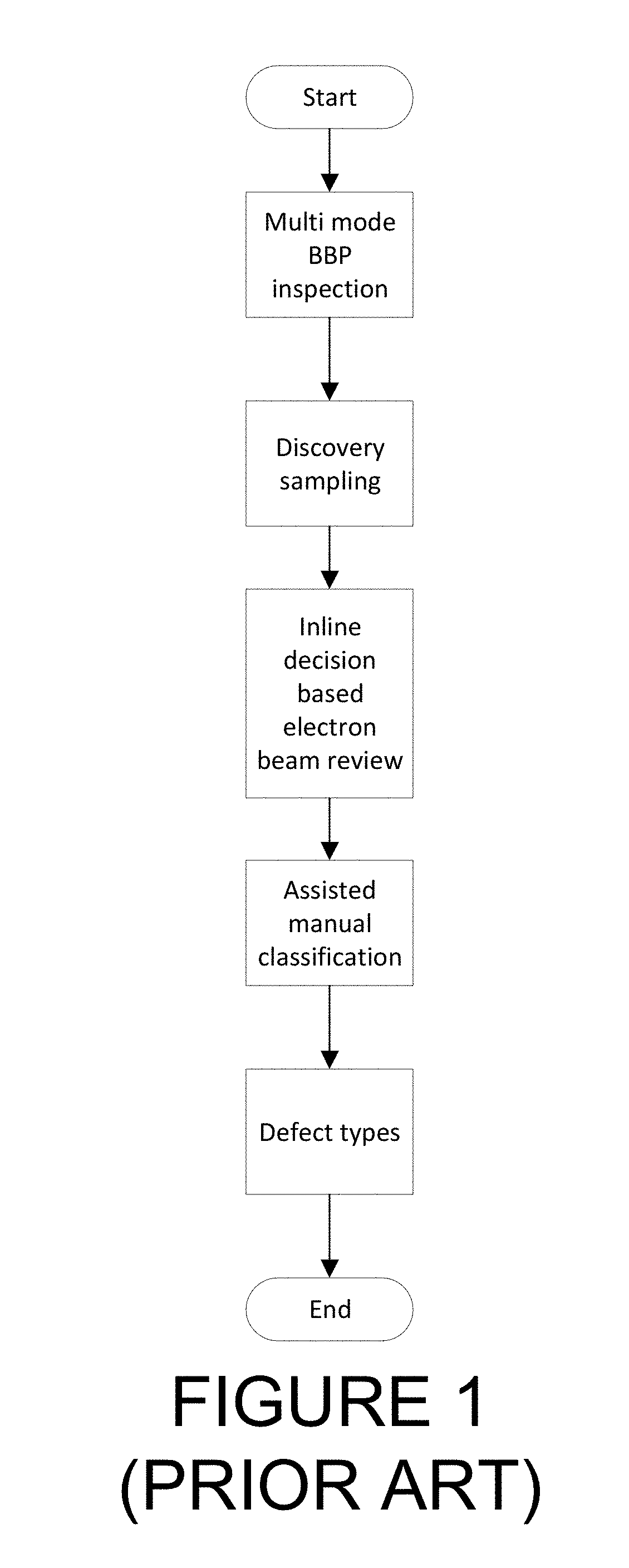
First, it may take one to two days to find all the defect types using the previous technique.
There is an extremely high nuisance rate in the BBP inspection scan, which can lead to difficulty when performing deskew when a design is not available.
Optical inspection gap defects also cannot be discovered.
There is no real-time intelligence to vary inspection or sampling based on already-identified defect types.
Inspection scans have a low defect count, leading to higher de-skew time on the SEM tool, which can be upwards of two hours.

Method used


Image

  • Defect discovery using electron beam inspection and deep learning with real-time intelligence to reduce nuisance
  • Defect discovery using electron beam inspection and deep learning with real-time intelligence to reduce nuisance
  • Defect discovery using electron beam inspection and deep learning with real-time intelligence to reduce nuisance

Examples


Embodiment Construction

[0029]Although claimed subject matter will be described in terms of certain embodiments, other embodiments, including embodiments that do not provide all of the benefits and features set forth herein, are also within the scope of this disclosure. Various structural, logical, process step, and electronic changes may be made without departing from the scope of the disclosure. Accordingly, the scope of the disclosure is defined only by reference to the appended claims.

[0030]Defect discovery an important production step for semiconductor foundries. It reduces time-to-product and can help with ramp-up. The present disclosure provides for defect discovery using an inspection or review system, such as electron beam inspection, and deep learning with real time intelligence to reduce nuisance. Defect discovery with electron beam inspection tools can be improved with deep learning to speed up the process. Embodiments of the present disclosure increase the efficiency of defect discovery by usi...


PUM


Abstract

A deep learning algorithm is used for defect discovery, such as for semiconductor wafers. A care area is inspected with the wafer inspection tool. The deep learning algorithm is used to identify and classify defects in the care area. This can be repeated for remaining care areas, but similar care areas may be skipped to increase throughput.

Description

CROSS-REFERENCE TO RELATED APPLICATIONS[0001]This application claims priority to Indian Provisional Application No. 201841000585, filed on Jan. 5, 2018, and U.S. Application No. 62 / 636,032, filed Feb. 27, 2018, the disclosures of which are hereby incorporated by reference.FIELD OF THE DISCLOSURE[0002]The disclosure generally relates to semiconductor inspection. More particularly the disclosure generally relates to methods for efficiently discovering defects based on prediction.BACKGROUND OF THE DISCLOSURE[0003]Evolution of the semiconductor manufacturing industry is placing ever greater demands on yield management and, in particular, on metrology and inspection systems. Critical dimensions continue to shrink. Economics is driving the industry to decrease the time for achieving high-yield, high-value production. Minimizing the total time from detecting a yield problem to fixing it determines the return-on-investment for a semiconductor manufacturer.[0004]Fabricating semiconductor dev...

Claims


Application Information

Patent Timeline
Patent Type & Authority Applications(United States)
IPC IPC(8): G06T7/00G06K9/62H01L21/66H01L21/67G06N99/00G06V10/764
CPCG06N20/00G06T7/0006G06K9/6267H01L22/12H01J37/28H01J37/244G06T2207/30148G06T2207/20081H01L21/67288G06T7/001H01L22/20G06N3/08G06N20/20H01J2237/2817G06T2207/20084G06V10/82G06V10/764G06N5/01H01L22/30G06F18/24
Inventor YATI, ARPIT
Owner KLA TENCOR TECH CORP
Learn More