Semiconductor structure and method of preparing semiconductor structure
- Summary
- Abstract
- Description
- Claims
- Application Information
AI Technical Summary
Benefits of technology
Problems solved by technology
Method used
Image

Examples
embodiment 1
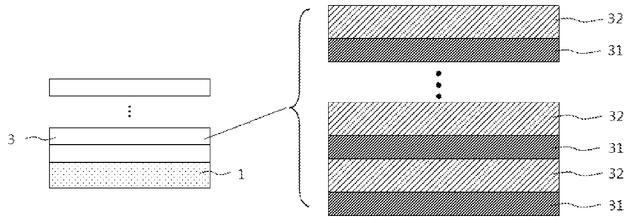
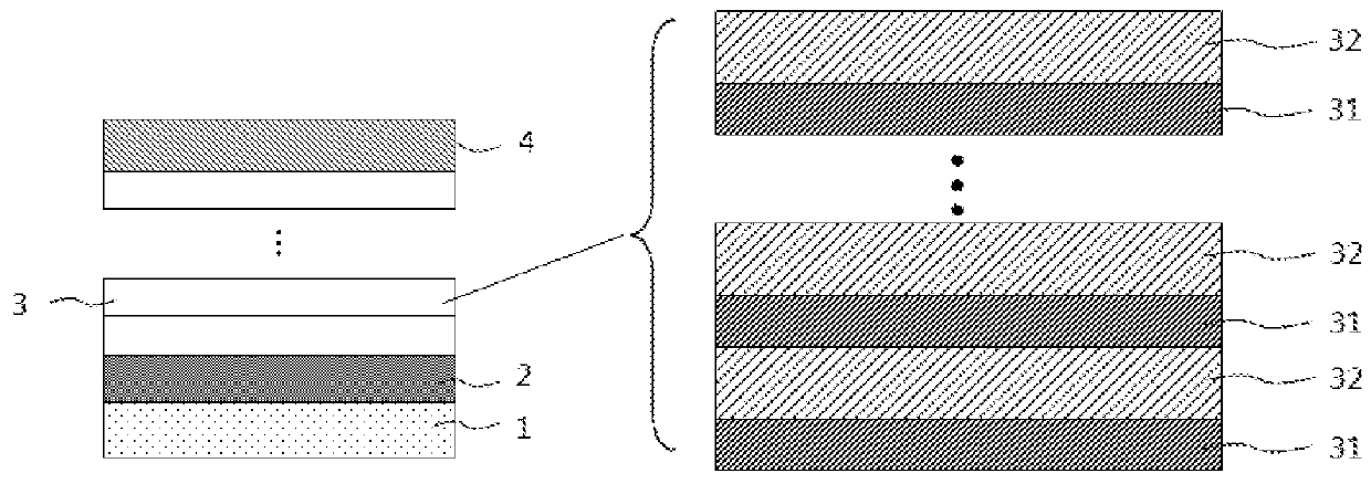
[0031]FIG. 1 is a schematic diagram of a semiconductor structure according to an embodiment of the invention. As shown in FIG. 1, the semiconductor structure includes a substrate 1, and at least one periodic structure 3 disposed above the substrate 1. Each of the periodic structures 3 includes at least one period, and each period includes a first periodic layer 31 and a second periodic layer 32 which are sequentially superposed in the epitaxial direction.
[0032]In an embodiment of the present invention, as shown in FIG. 2, in order to reduce the dislocation density and the defect density and prevent melt-back, the semiconductor structure may further include a nucleation layer 2 disposed between the substrate 1 and the first periodic structure 3. In another embodiment of the invention, in order to form a complete electronic component structure, the semiconductor structure may further include a component action layer 4 disposed over the at least one periodic structure 3. The active reg...
embodiment 2
[0041]When the thickness of periodic structure 3 along the epitaxial direction is increased by increasing the number of periods along the epitaxial direction, the thickness of the adjacent periodic structures 3 can also be independently adjusted. More specifically, in at least one periodic structure 3, the thickness of the first periodic layer 31 of the nth periodic structure 3 in the epitaxial direction may be greater than the thickness of the first periodic layer 31 of the (n+1)th periodic structure 3, the thickness of the second periodic layer 32 of the nth periodic structure 3 may be equal to the thickness of the second periodic layer 32 of the (n+1)th periodic structure 3; or, in at least one periodic structure 3, the thickness of the second periodic layer 32 of the nth periodic structure 3 in the epitaxial direction may be less than that of the second periodic layer 32 of the (n+1)th periodic structure 3, and the thickness of the first periodic layer 31 of the nth periodic str...
embodiment 3
[0067]An embodiment of the present invention provides a method of preparing a semiconductor structure. The method includes: preparing at least a periodic structure 3 above a substrate 1; wherein the materials of the periodic structures 3 are III-V group compounds, each periodic structure 3 includes at least a period, each period includes a first periodic layer 31 and a second periodic layer 32 which are stacked sequentially along an epitaxial direction; wherein the first periodic layer 31 includes a first III group element, a second III group element and a first V group element, the second periodic layer 32 includes the first III group element, the second III group element and the first V group element; or, the first periodic layer 31 includes the first III group element and the first V group element, the second periodic layer 32 includes the first III group element, the second III group element and the first V group element; wherein the atomic number of the first III group element ...
PUM
 Abstract
Description
Claims
Application Information
 - R&D Engineer
- R&D Manager
- IP Professional
- Industry Leading Data Capabilities
- Powerful AI technology
- Patent DNA Extraction
Browse by: Latest US Patents, China's latest patents, Technical Efficacy Thesaurus, Application Domain, Technology Topic.
© 2024 PatSnap. All rights reserved.Legal|Privacy policy|Modern Slavery Act Transparency Statement|Sitemap